 Haim Grebel
 Haim Grebel
Professor, Electrical and Computer Engineering
Director, Electronic Imaging Center, EIC@NJIT
New Jersey institute of Technology
Research Interests:
Linear and nonlinear properties of nanostructures
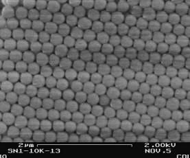
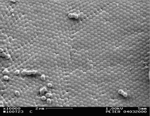
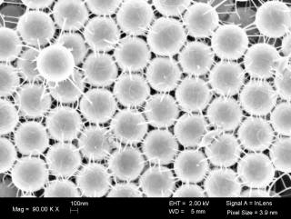
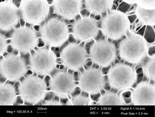
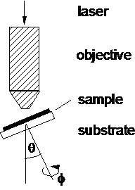
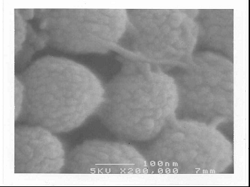
Left: Self-assembled 245-nm silica nanospheres. Right: These structures are later ion-implanted with Ge. Nanoclusters of the guest material, approximately 3-nm in size, are formed within the silica nanospheres following annealing at 1000oC. The final result is 'nano within nano'.
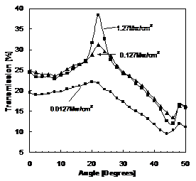
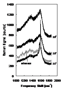
Linear transmission (left) exhibits a dip due to the periodic opaline structure. Transmission at various laser intensities is shown on the right. The structures have been ion-implanted with Si and Er ions as well.
Single Wall Carbon Nanotubes (SWCNT)
These are grown using Chemical Vapor Deposition (CVD) method
(a) (b)
(c)
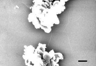
(a) Single-wall carbon nanotubes (SWCNT) grown in the voids of an artificial opal.
(b) This enabled us to wrap them with semiconductive polymer and (c) study individual tubes
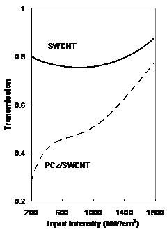
Nonlinear transmission through SWCNT imbedded, order array of silica spheres. Upper curve - with only SWCNT. Lower curve - electrochemically wrapped SWCNT with polycarbazole. The laser used was 25 ps Nd:YAG at l=1064 nm.
(a) (b) (c)
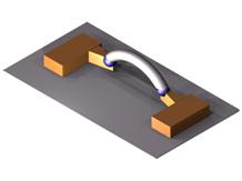
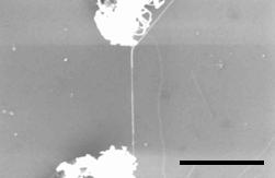
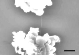
Individual CNT interconnects. (a) The structure. (b) Electrode layout. (c) A bridge spanning between the electrodes (the bar length is 1 micron)
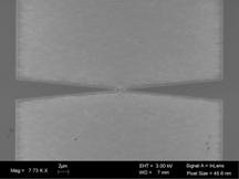
Rectifying a CNT interconnect. Left: Bent Interconnect. Right: Rectified interconnect after applying 1 V. (the bar is 1 micron)
High-pressure phases (hex-Si, hex-Ge, hex-diamond) formed by use of laser ablation
Silicon and germanium are most likely to form cubic phases under normal equilibrium conditions. At high pressures, Si or Ge may possess other crystallographic symmetries. Using laser ablation technique we were able to grow stable phases seen only at very high pressures (~10 GPa).
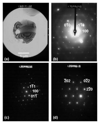
(a) Hexagonal-Si (hex-Si) crystal. (b)&(c) Electronic diffraction patterns from hex-Si. (d) Electronic diffraction pattern from cubic-Si (c-Si).
Infrared Filters
Infrared filters are forms by stacking two-dimensional metallo-dielectric screens in order to achieve three-dimensional structures. Each screen has a resonating behavior at long wavelengths (longer than the feature size) and by stacking them one enhances their transmission or reflection characteristics. Metal screens with opening are called inductive screens; dielectric screens patched with metal features are called capacitive screens.
Photonic crystal made out of metallic screens
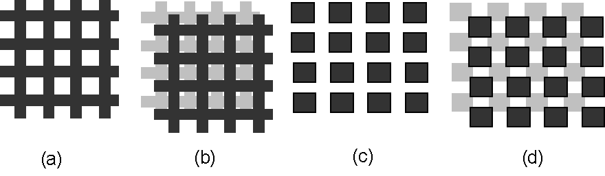
(a) Aligned openings of two inductive screens and (b) non-aligned. Similarly for capacitive screens,
(c) aligned and (d) non-aligned.
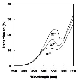
Transmission Curves
![]()
(a) Simulations for 4 inductive screens at spacing of ¼ resonance wavelength. Thin line: non-aligned, bold: aligned. (b) Four capacitive screens at spacing of ¼ resonance wavelength. Thin line: non-aligned, bold: aligned.
Surface Enhanced Raman
Left: Surface Enhanced Raman Spectroscopy (SERS) with silver coated opaline structure. Middle: A suspension with CNT is placed on the platform. Right: The Raman signature of SWCNT clearly appears when the sample is tilted such that surface plasmons are excited (25o in this example).
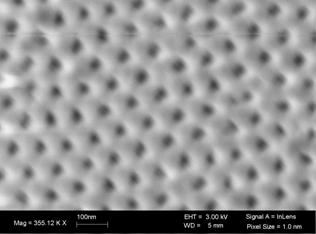
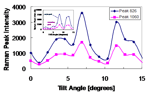
Similarly, one may explore enhanced Raman scatterings with array of holes. Left: An array of holes in anodized aluminum oxide. The hole pitch was 90 nm. Right: The peak intensity is increased when the sample is tilted. Shown are two Raman lines from B. subtilis (a known Anthrax simulant). The inset exhibits Raman peak enhancement for SWCNT.
Infrared systems (Electronic Imaging Center)