Reliability
of Low Power Nano-Devices with High-k Gate
Dielectrics
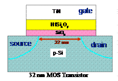
Because of the implementation hafnium (Hf) based high-k dielectrics for sub-45 nm CMOS technology
nodes to reduce power while making the devices faster, there has been a lots of
activities to further understand the durability of these nano
devices. These high-k dielectrics in active nanosystems
provide distinct advantages of thermal stability and leakage characteristics.
Our group has identified the inherent
energy levels of the electrically active ionic defects within the bulk high-k
experimentally as a part of the reliability study of these dielectrics. We used
low temperature and leakage measurements to identify the defects in the context
of MOS device energy band diagram for the first time in Hf-based
gate stacks. We have also established an excellent match between experimental
and calculated defect levels to understand the device performance. It shows
that oxygen vacancies are responsible for electron trapping at both shallow and
deep levels thereby degrading the electron transit in the device. To compensate
the mobility degradation our group is depositing Hf-based
dielectrics directly on alternate high mobility Ge substrates by collaborating
with IBM. These devices are found to be too leaky and show significant
hysteresis due to the formation of unstable interfacial layer of GeO2 during the deposition. Therefore, interfacial treatments like Ge
surface nitridation prior to gate dielectric
deposition is used to understand the effect of surface nitridation
on interface as well as on bulk dielectric.
Results
from negative bias temperature instability (NBTI) studies under low bias
conditions and at elevated temperatures show that interface state generation in
pMOSFETs is quite low at low bias conditions whereas
at high bias conditions significant interface state generation was observed. In
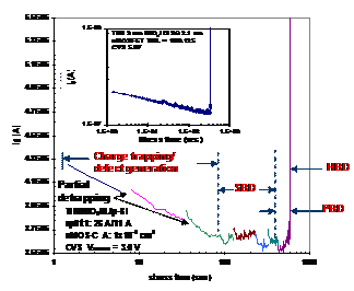
a breakdown study for these gate stacks with multiple dielectric layers,
constituting a thin interfacial layer of silicon dioxide and the high-k layer,
with a metal gate his group found that the interfacial layer is responsible for
the gate stack breakdown. Our group also observed that how the interfacial film
determines the nature of degradation. This work is carried out in collaboration
with International SEMATECH,
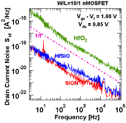
We have a strong collaboration with IMEC, Belgium for his research
work in the area of 1/f noise measurements in high-k gate dielectrics as a
function of several metal oxide semiconductor (MOS) gate processing parameters,
such as thickness of the interfacial layer and the high-k oxide, bulk
properties of the high-k layer, high-k deposition technique, percentage of
hafnium content, post deposition anneal (PDA) treatments, choice of gate
electrode material (poly-silicon, fully silicided or
metal) and gate electrode processing. Low frequency noise diagnostics is a
powerful tool for device performance and reliability characterization.
In a recent
project in collaboration with NASA we have designed and fabricated a wafer-level thinned CMOS image sensor implemented in a
bulk-CMOS technology. The imagers were radiation hardened by annealing in
deuterium for space application. Our research group’s
cental focus is in the Material Characterization
working in the areas of VLSI devices and processing and integrated sensors.