This document contains a step-by-step tutorial for creating an inverter in the Mentor Graphics application Design Architect. It covers entering the schematic, creating a symbol, and creating a viewpoint. Separate documents continue the tutorial for other Mentor applications.
The first thing that we need to
do to begin the circuit design process is to capture our schematic in
Design Architect, referred to as DA. You will use N-FETS and P-FETS
from a special library as these components have the necessary properties
assigned to drive the entire process. After placing these FETS, you can
wire them together and add ports and net names as you would any other
design. You can even create hierarchical designs and then design your
layout from that.
ADK
(ASIC Design Kit) is an add-on to Mentor that does a lot of the work for
us. For current project we
will use many of the ADK features, including schematic libraries with
basic elements (transistors, VDD, etc.) and several standard gates. The basic elements for transistor
level design are in the SDL Library.
You should use these elements for all transistor level design.
Cells
in the ADK library are sized (W & L) in units of 'lambda', not
microns. We will be using the
0.35um process with a lambda of 0.2, so if you set L=2 you will
get
a length of 0.4um.
To start DA, type
> mentor adk_daic &
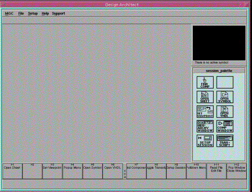
This command will load DA with a special library available that contains all the parts you will need for capturing your designs. The '&' at the end of the command will allow you to enter commands in the terminal window after DA starts running. Once DA is running, you should see the window shown in Figure 1.

To begin a new design, you must
open a new sheet from the DA menu bar. Select
File > Open
> Sheet
(Alternatively, you can click on OPEN SHEET
on the side menu). Enter the name of your
cell in the Component Name slot. Do not change the
value of the Sheet slot. Since we want to create an
inverter, call the cell inv, as shown
in Figure 2. Click on OK and a
new blank sheet will open.
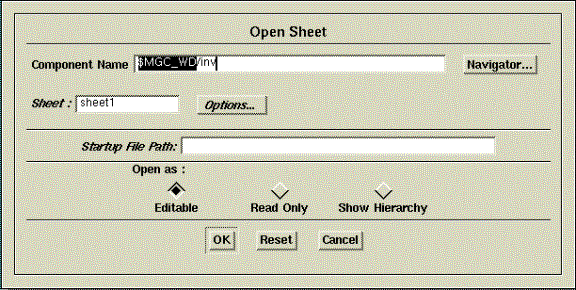
Figure 2
 Now we can use transistors to draw an inverter
gate. To find pmos and nmos transistor, from the top menu select
Libraries >
ADK Libraries
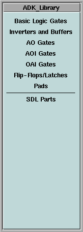
which will show the ADK Libraries palette
menu on the right of your Design Architect window, as shown here to the
right.
The top six entries in this
palette will give you a list of standard cells that you can use from the
supplied library. You will use these libraries in your later
design. The last item, SDL Parts, will give you
another palette menu with the basic parts you will use to build your
custom design circuit.
Click on
SDL Parts to show the SDL Parts palette
menu.
Locate the transistors form this palette menu named
n-fet-4 for nmos and p-fet-4 for pmos. Note that
these transistors are four-terminal transistors which include a body
(substrate) terminal. When you draw a circuit, you must connect
nmos body to GND and pmos body to VDD.
Add
transistors to your schematic. Select an nmos device from
menu and place it into the inv schematic window as shown in
Figure 3. Next, place a pmos device into the window. You can
see the instance (part) that you place in the window is highlight, which
means this instance is selected and will be affected by the next
operation. You should de-select the instances you've added by
pressing the F2 key.
Notice that
all Mentor app have many basic commands programmed into the
function-keys. Study the menu at the bottom of the screen and
notice that commands are also listed for shift, alt, and ctrl
combinations with the function-keys. You will want to use many of
these shortcut keys to simplify your work and should practice them on
your own. For now, we will only point out F1 and F2 which are used
to select and deselect.
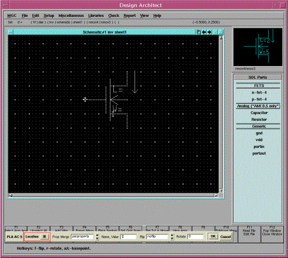
Figure 3
Add power
ports to your schematic by selecting and placing the vdd
and gnd instances from the SDL Parts palette
menu.
Next you need to add an input and output port. Select and
place the portin and portout parts from the SDL Parts menu. Note that
these parts are on the SDL palette for your convenience, but are not
specific to the ADK; you can use ports from any of the libraries.
After putting all components that you need into schematic window, press
Esc to cancel the place parts operation. Note that you
should always remember to press Esc to exit each operation when you are
finished with that operation.
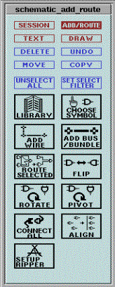 Right-click on the palette
menu (which should currently show the SDL Parts library) and
select
Display
schematic palette
This will take you back to main palette,
which is shown here on the right. You can edit your circuit by
using this palette.
to add the appropriate wire connections to
your schematic.
Now, move
the instances around to get them in the proper position for an
inverter, VDD on top, then pmos, then nmos, etc. You can move the
instances by selecting each instance individually and
selecting
MOVE
from the main schematic palette.
When the instances are
in the proper location, you can add wires to connect your circuit.
From the main palette, select
ADD
WIRE
and wire your circuit by clicking at each wire node
and double-clicking to end a wire. Remember, you will be in the
ADD WIRE operation until you hit Esc.
Next, you should name the
input and output ports. From the main palette, select
TEXT >
CHANGE VALUE
and then clicking on the appropriate
port. Enter the name of the input port
as in and repeat the procedure to name
the output port out.
The default W/L value of the
MOSFETs from ADK library is 5/2. To change the size of the
transistor, hit F2 to deselect everything,
select a transistor, and then right-click over the transistor. A menu will
pop up showing yet another way to access commands in DA. Select
Properties > Modify
and the the property you
want to modify. For this tutorial, change the
width of the pMOS transistor to 10 (for 10l = 3mm).
Now the schematic of the
inverter gate is finished and should look similar to the one in Figure
4. Before saving your cell, you need to check the sheet. You
can access the command from both the main DA menu or by right-clicking
on the background of the sheet. From the main menu select
Check >
Sheet > With Defaults
If you have any errors, be sure
to fix them before continuing. You can expect to get a few
warnings which you can ignore, but you can't ignore errors.
Once you have successfully
checked your sheet you can finally save the
cell. Select
File > Save
Sheet > Default Registration
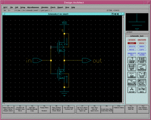
Figure 4
Like most circuit design CAD software, Mentor Graphics provides for hierarchical design, which means that you can instantiate your lower level cells (circuits) into upper level cells to create a tree structure. This allows you to create each basic cell only once and then use it over and over again by adding it to other cells (called, instantiating -adding an instance, or cell). Since, at higher levels, we really don't need to see the detailed transistor-level description of the base cells, we create symbols which will appear when we add the cell to higher-level cells. Generally, it is preferred to have the symbol appear in a way that represents the function of the cell, like using standard gate symbols for inverters, nands, nors, etc. The following will explain how to create a symbol for your inverter and how to make it look like an inverter.
1.
While still in DA, from the main menu select
Miscellaneous > Generate Symbol
to automatically
generate a symbol. Do not change any of the options in the dialog box and
click on the 'OK' button to generate a symbol
for your cell. The generated symbol will be a simple rectangle with
two pins, IN and OUT, which does not look much like an inverter, so we
will modify the appearance of this symbol.
2.
To make your inverter symbol look like an inverter:
- Select the
body (rectangle) of the symbol and delete it. Dont delete the two pins of
the symbol.
- Click DRAW à
ADD POLYLINE and draw a triangle as shown in Figure 5.
- Click
DRAW à
ADD CIRCLE to draw a circle at the front of the triangle.
-
Press F2 to unselect these shapes.
- Individually select the two Pins,
and click MOVE to move them to the proper position relative to the symbol
you have drawn.
- Because this symbol is small, it will look much
better if we place the pin text outside of the symbol (this is an optional
step -just makes your symbol look better). Click TEXT à
CHANGE VALUE, select pin names, and then click MOVE to move pin
names to proper position as shown in Figure 6.
- Choose File
à Save Symbol to save the symbol.
3.
To further identify you cell, you can add the name of the cell on
the symbol so that it will show up when you instantiate it. To do
this, from the main menu select
Edit > Add
Graphics > Text
and type INV as
the text. Place this text in the symbol. You can use the move
command to move it around as suits you.
4.
To finish, we need to check the symbol for errors. From the
main menu
select
Check > With Defaults
You can
ignore the warnings about the properties not being on the interface. If
you have any other errors, however, you need to fix them before moving on.
5. Save your
symbol by selecting
File > Save
Symbol > Default Registration
6.
Close the symbol window by clicking on the X in the upper right
corner of the window.
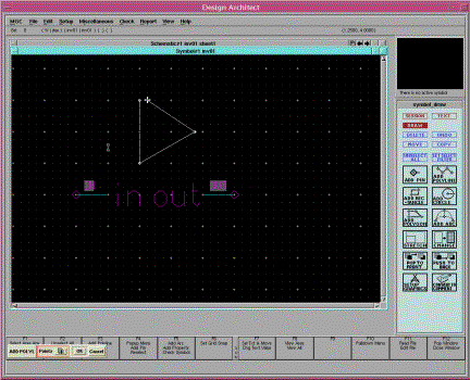
Figure 5
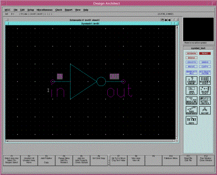
Figure 6
To simulate your circuit with QuickSim, AccuSim and go on complete the layout of the circuit, you should create a viewpoint of your circuit. A viewpoint is similar to a netlist and is used by the other Mentor Graphics applications are a representation of your circuit. This step is very simple.
1. Minimize your Design Architect window (use the icon on the upper right of the DA window),
2. Type following command
at a terminal prompt (you must be in the same directory as your
cell),
>adk_dve
<cellname> -technology tsmc035
Here filename is
inv.
OK! The schematic entry is
done. Now you are ready to
check your schematic with the signal simulator, Accusim or HSpice.