xij = <ViV*j>
where Vi
is the complex voltage from antenna i,
and Vj
is the complex voltage from antenna j.
This can be made a function of delay τ,
by writing
xij(τ)= <Vi(t)V*j(t+τ)> , (1)that is, we delay Vj(t) by a time τ and do the correlation (i.e. multiply and then integrate). Note that correlation is commonly used to find time delays in two waveforms, as seen in the figure below, from Hanaoka (1999):
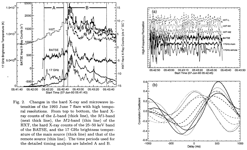
Figure 1: Example of a cross-correlation to establish the time lag between two waveforms, in this case due to solar bursts measured
in different wavelengths (hard X-rays and radio waves). The panel (b) shows the result of cross-correlation of waveforms in (a).
When Vi(t) and Vj(t) have a finite bandwidth, the delay pattern looks like this:
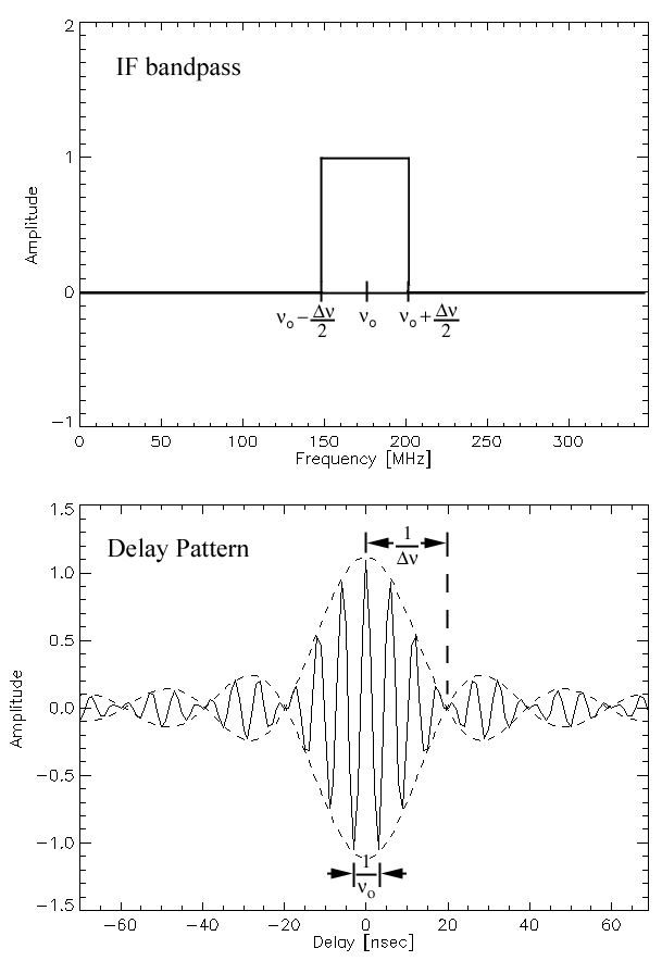
Figure 2: The relationship between the IF bandpass of each antenna and the delay
pattern in the cross-correlation of signals from two antennas. The upper panel
represents the spectrum of the signal Vi(t) (equation 1) from one antenna, and the
bottom panel represents the cross-correlation in eq. (1), xij(τ)= <Vi(t)V*j(t+τ)>.
The relationship between them is just the FT relation.
where the Fourier Transform
of the IF bandpass gives the delay pattern. Note that the overall
delay pattern is a cosine wave with period 1/νo,
modulated by a sinc pattern of width 1/Δν.
This is a case where we could use what we learned in Lecture 6,
AB = A * B (convolution theorem)
A * B = A B .
Looking at the second equation, we can consider the square bandpass as a function A, which is a squarewave centered at ν = 0, convolved with a function B, which is a delta function at ν= νo. The FT of this convolution is the product of the individual FTs, i.e. A, which is a sinc function, times B, which is a cosine function. So the convolution theorem really works!
For the Owens Valley Solar Array (OVSA), we need to determine the delay centers frequently, to ensure proper operation. This is done by observing a strong source and sweeping the delay through a range of values to find the peak of the delay pattern, which gives the optimum delay. (Will look at DLASCAN in I3542055.ARC) It is important that the delays in the system that correct for different cable lengths be known and compensated for, otherwise the amplitude of the correlation suffers considerable loss of efficiency. Once we know the delay centers (delays needed to correlate a source directly overhead), then it is easy to calculate the correct delays for any other location in the sky, i.e. the geometric delay τg= B . s/c. (Will look at Gelu's writeup on delay pattern, including phase.)
Last time we briefly mentioned digital correlator design, and discussed the two alternatives, FX and XF. Let's repeat that in a little more detail. Recall that a single baseline gives a response as shown in Figure , below:
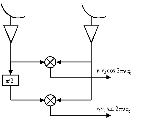
Figure 3: Inserting
a phase shift of π/2
in one of the antennas and doing a
second correlation allows
both sine and cosine components to be measured
simultaneously. These
are recorded and become the complex visibility at
spatial frequency u,v
corresponding to the projected baseline between the antennas.
XF Correlator
We can combine the outputs
into a single complex expression,
xij(τ) = <Vi(t)V*j(t+τij)> = <Ai(t)A*j(t+τij)> exp(i2πνoτij) (2)
where we write the geometric delay for baseline i-j as τg = τij, νo is the local oscillator frequency, and Ai(t) is the slowly varying amplitude that, in figure 3, is written as vi (integration represented by the <> brackets is implied in Figure 3). The exponential term in equation (2) represents a time variation that can be calculated from geometrical considerations and removed in software. Now the delay pattern in Figure 2 is obtained by slowly sweeping the geometric delay from below to above its optimum value, which takes of order 1/2 hour at OVSA. However, one can imagine delaying the signal in unit steps and doing many correlations simultaneously, to obtain the lower panel of Figure 2 instantaneously. Then one can do the inverse FT and obtain the cross-power spectrum. This is the function of an XF, or lag correlator, which first does many correlations (the X part) and then does a FT (the F part). The goal is to get the visibilities for baseline i-j as a function of frequency. Note that OVSA does not do this, hence it obtains the visibility only at the optimum delay (zero lag), and is therefore called a continuum correlator. Figure 4 shows the X part of an XF correlator block diagram, which would then be followed by a hardware FFT:
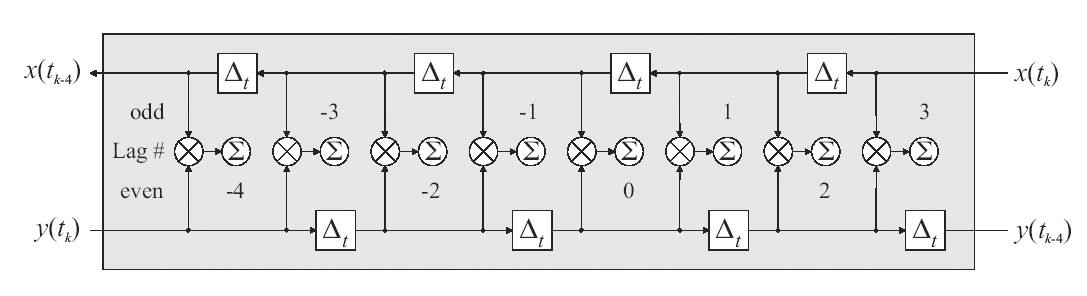
Figure 4: A lag correlator design. Note that the two antenna inputs come from opposite sides of the device, which allows
for a symmetric design. The total lag between signals at each correlation is nΔt, where the integer n is shown in each block.
The S symbols denote integration. The output of each integrator is then xij(τ)then, from equation (2). The FT of xij(τ)
(not shown) gives the cross-correlation spectrum.
It is interesting to look at a little more detail of how such a correlator might be implemented. Figure 5, below, shows the block diagram of a larger part of the system, where the antenna signals x(t) and y(t) are digitized, then entered into "time demultiplexers," which are essentially shift registers. The data enters serially, so is at a high clock speed, but exits in parallel, so the correlator chips can operate at a lower clock speed. Each block labeled CC below, represents the entire lag correlator function shown in Figure 4, above, so they essentially subdivide the time between the correlator chip clock cycles. As an example, say the digitizer is operating at 1000 MHz, and the time demultiplexers are 8-bit shift registers. The data come in at 1000 MHz, but go out at 1000/8 MHz = 125 MHz. Each line out of the time demultiplexer then represents a delay of 1/125 MHz = 8 nsec. The delays Δt in Figure 4 would then be 1 nsec each, and the correlator chips CC would give 8 lags. The total number of lags for each clock cycle of the larger block would be 64 lags.
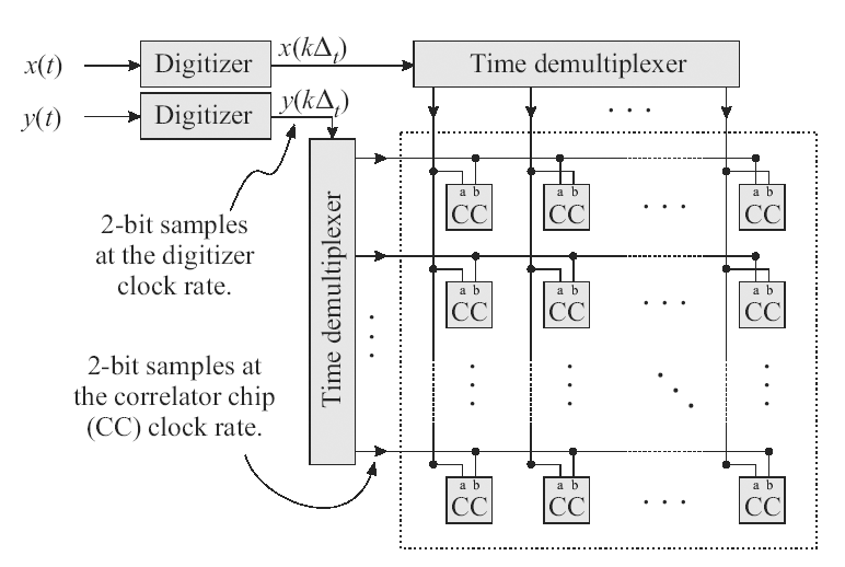
Figure 5: A larger part of the digital system, showing the digitizer step, and how the correlator chip, CC,
shown in Figure 4 fits into the overall scheme. Historically, each CC block would be done on a single IC
chip, designed for this special purpose and mass produced as an ASIC. The entire 8x8 area shown
by the dotted line would be a printed circuit card. Note that this electronics performs the correlation
for only a single baseline. For an array of N antennas, N*(N-1)/2 cards would be required. More recently,
the entire block can be implemented on a single giant FPGA (Field Programmable Gate Array) chip,
whose function can be programmed using the VHDL language, much like writing software.
We should also note that the lag correlator can be used to do autocorrelation, where a signal from one antenna is correlated with itself (suitably lagged). After FT, this gives the auto-correlation (also called power) spectrum (and is a real quantity rather than a complex visibility).
Fractional Delay Errors
In any design, the geometrical
delay must be compensated. For OVSA, this is done by switching
in variable lengths of cable (called analog delay compensation), while
in digital systems we can accomplish the same by using digital delays.
In either case, the delays are quantized to some minimum step size. For OVSA, the delays are
quantized to 1 nsec (equivalent to about 1 foot cable sections).
For the Caltech mm-array, operating at much higher frequency, the delays
are quantized to 1/128 nsec! Say we have a system with 1 nsec minimum delay step, and
that the system is set for perfect delay at the center of the sample.
Then the delay will be off by a fractional time −ε/2
nsec at the start of the sample period and +ε/2
at the end of the sample period. For a wideband signal, this introduces
a phase shift across the band that varies with frequency within the band,
as can be seen from equation (2), i.e.
xij(τ) = <Vi(t)V*j(t+τij)> = <Ai(t)A*j(t+(εi - εj))> exp(i2πνo(εi - εj)) (2')
If uncompensated, the amplitude at the high frequency end of the band would be depressed. For this reason, correlators are often designed to incorporate phase rotation compensation, which is to say they shift the phase of the incoming signal both positively and negatively during the delay digitization period. This must also be quantized, and the accuracy depends on the number of bits of the correlation. For a three-level correlator, the phase rotator has three states, +φ, − φ, and 0.
FX Correlator
As we mentioned last time,
an FX correlator does the same job as the XF correlator, but inverts the
FT and correlation (X) functions, doing the frequency division first.
It is perhaps simpler, conceptually. The idea is that the incoming
signal is divided up into different frequencies using a filterbank, and
each of these signals is then correlated with all of the signals at the
same frequency among all of the other antennas. No lags are required,
so the correlation job is simpler--each is essentially a continuum correlator.
The phase correction due to delay errors is also a simpler job, because
one simply has to shift the phase of each frequency channel in the appropriate
way. The frequency division can be done with an FFT, but note that
the frequency resolution of such an FFT is related to the number of samples
being transformed. Fine frequency resolution requires a long time
series. Even then, the Gibbs ringing phenomenon causes some problems,
notably blending of signal into adjacent channels. There is a relatively
new development called polyphase filters, which has better characteristics
in this regard, and can divide the incoming signal more cleanly into sub-bands. This approach was developed for "frequency-domain multiplexing" in wireless communications systems. Figure 6, below, shows an overview of the procedure. The key is that this procedure can be implemented in hardware and can keep up with the data flow rate.
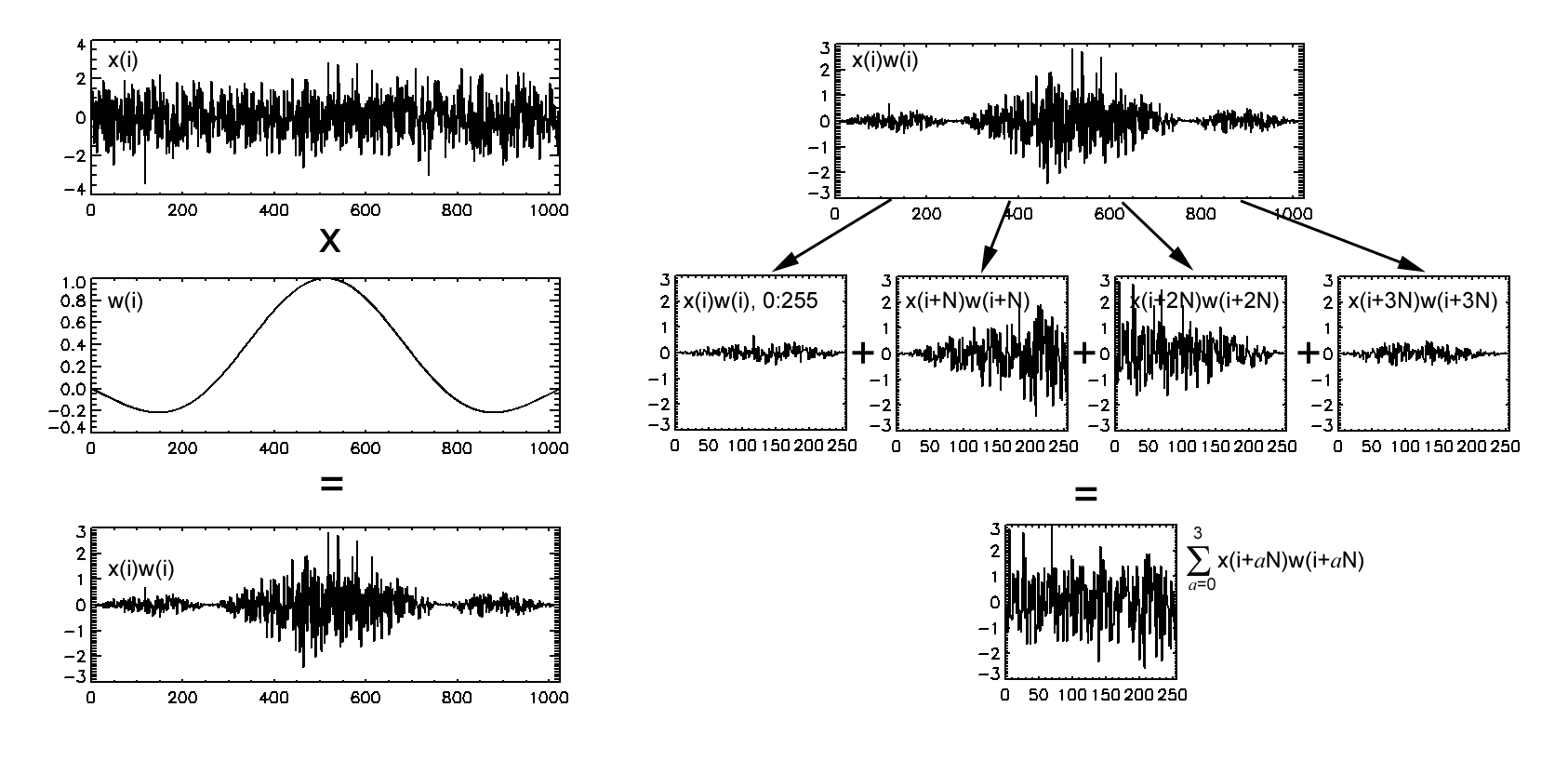
Figure 6 : A graphical representation of the polyphase filter process. A time series of some length (here shown as 1024 samples,
is multiplied by a "window" function that is a sinc function
(because of its property that its FT is a rectangle function) to yield
the waveform shown in the lower left. The windowed samples,
repeated in the upper right, are split into n separate sections (here
shown as 4 sections, therefore each of length 256), and the
resulting
sections are summed to yield the final waveform in the lower
right. This waveform is Fourier transformed to give a
spectrum with a nice, rectangular bandpass.
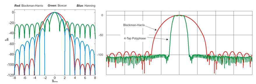
Figure 7 : A comparison of the performance of various windowing functions and the FFT (green curve in plot at left).
The two figures of merit are the width of the "channel" and the height of the side-lobes on either side. The higher the
sidelobes, the greater the "cross-talk" between channels. The FFT sidelobes are only 20 dB below the main peak,
while for the polyphase filter profile (green curve in the plot at right) the sidelobes may be down by more than 100 dB.
The rectangular bandpass and low sidelobes approach the ideal.
Figure 7 shows the performance of the polyphase filter compared to the FFT and some other windowing functions.
The Frequency Agile Solar Radiotelescope may use an FX correlator design in order to solve the problem of interference. In an XF correlator, some broadband signal is cross-multiplied, and then Fourier transformed. In the presence of narrow-band interference (say some communication channel), the signal levels for the entire band may be quite high, saturating the digital electronics of the correlator. This destroys the measurement for all frequencies in the band. This can be overcome by using a many-bit correlator, but this means that every CC chip in Figure 5 has to operate on many bits, which is expensive. By using an FX correlator, one can digitize to many bits, and then channelize the input band into many sub-bands. Those channels with interference can then be removed and not correlated at all, while those without interference will have low amplitudes (relative to the interference channels), but can be sampled at much lower bit resolution (perhaps a 2-level, 1 bit comparator). The subsequence CC chips can all be 1 bit chips, making the implementation very inexpensive. The reason FASR faces this problem more than previous arrays is that it will operate over a very large bandwidth, and so will operate in parts of the radio spectrum where strong interference exists. Other new arrays (EVLA, ATA, LOFAR, SKA) are also facing the same challenges.
Spectral Line Imaging
Issues
See the lecture
by Michael Rupen on Spectral Line Observing I at the NRAO Summer School. In order to do spectral
line work, one must determine the individual bandpasses on each baseline
(both amplitude and phase) and correct for the nonuniformities. One
can then image at each point in a spectral line, and obtain a "data cube"
containing two spatial and one spectral dimensions.