Go to COE394 Experiment | 1 | 2 | 3 | 5 | 6 | 7 | 8 | 9 | ECE Lab home
![]()
|
Go to COE394 Experiment | 1 | 2 | 3 | 5 | 6 | 7 | 8 | 9 | ECE Lab home |
|
COE394 - Experiment 4
Programmable Logic Devices
1. Introduction
As IC fabrication technology advances, new chips are created which can perform the functions of several ICs. This is desirable because it reduces board space and power requirements, facilitates debugging and often reduces propagation delay. The technology in question is generally referred to as ASIC (Application Specific Integrated Circuits). The process of designing and fabricating ASICs is expensive, and is usually justified only for large production runs. Techniques involving EPROMs and PLDs can be used at the design-bench even by small operators. In this experiment, the students will use the Altera EPM7128.
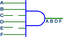
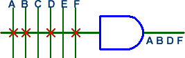
Before beginning the explanation of PLDs, it is necessary to become familiar with some new notation. Fig. 1(a) shows the logic diagram of a four input AND gate. Since a PLD can have AND gates with many inputs (32 in one case), the notation has to be modified as shown in Fig. 1(b). Each of the variables A, B, C, D, E and F can be an input to the AND gate if its fuse is left intact. An intact fuse is indicated by an X. Clearly, variables C and E are not inputs to this AND gate.
|
|
|
|
(a) |
(b) |
|
Fig. 1. Conventional logic notation (a) contrasted with more compact PROM and PLD notation (b) |
|
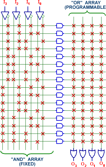
The first fusible link technology was applied to memory devices, such as field Programmable ROMs. The PROM can be used to implement combinatorial logic. Some pin saving can be obtained by using a chip design which is not quite as general as that of the PROM. That is the function of the PLD. To get an understanding of the difference between PROMs and PLDs, carefully examine Fig. 2.
Fig. 2. PROM architecture (a) compared with PLD architecture (b)
(a)
PROM
16 Words x 4 Bits
(b)
PAL
4 In - 4 Out -16 Products
In the PROM the AND array inputs are fixed. The sixteen AND gates shown produce all possible minterms of (I3, I2, I1, I0). During the programming phase the designer has the freedom to choose which minterms are ORed into each of the four output OR gates. During the programming phase some of the connections to the OR gates are removed, leaving in place only those desired. Suppose we need one combinatorial PROM output given by O3 = I0. This has to be implemented by using the sum of minterms given by
There is no point in reducing a logic function to its minimum number of terms, since the output is the sum of minterms in any event.
As can be seen in Fig. 2(b), the PLD has a fixed OR array and a programmable AND array. To get the same function O3 as discussed previously, it is necessary to program the inputs to the topmost AND gate. This is done by removing all the links used for ANDing normal and complemented versions of I3, I2 and I1. In addition, the link for ANDing
is also removed. All the links are left intact for the second, third and fourth AND gates. In this manner every variable is presented to the input of each of these AND gates in both normal and complemented form, so these gates will have outputs of zero. This way they will have no effect on O3.
The PROM realization utilizes eight 8-input AND gates and one 8-input OR gate to get the function O3. In the PAL realization we need only four 8-input AND gates and one 4-input OR gate. This saving in IC hardware can be put to use in implementing other desirable functions on the chip.
There are two basic types of PLDs. A combinatorial PLD, as its name implies, generates its outputs solely as a boolean function of its inputs. It allows feedback from any output to any AND array, and has tri-state buffers on its outputs. A registered PLD contains registers at its outputs. This is useful in designing sequential circuits, whose outputs and next state are a function not only of the inputs, but also of the current state.
In this experiment the EPM7128 will be used. The EPM7128 has up to 68 inputs or 64 outputs; each output has a separate output enable. The EPM7128 contains 64 macrocells. Each output can be programmed separately as combinatorial or registered outputs. The diagram of a typical macrocell is shown in Fig. 3.
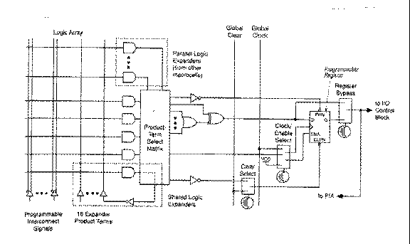
Fig. 3. Typical macrocell
2. Altera MAX+PLUS II Design File
The Altera MAX+PLUS II system has several methods for entering designs. In this experiment you will use the text entry method. In this method, the user creates an ASCII file (with the extension .TDF) which uses the Altera Hardware Description Language, AHDL. The format of this file is as follows. The sections in square brackets are optional, and the sections in braces are optional unless required by the design.
Each section is described below.
[Title Statement] This is the name of the design. This system does not require a header section.
If desired, the user may include this information in a comment field, which is delimited by a leading and a trailing percent sign (%).
[Constant Statement] This defines specific values and assigns them to symbolic names.
{Function Prototype Statement} This is used to define functions, their inputs, outputs and bidirectional ports. If you think of a function as a subroutine, the function prototype statement is used to declare the input and output variables of the subroutine.
{Include Statement} This allows the user to include other files in the AHDL file. This is especially useful for including macrofunctions in the design. Macrofunctions are predefined components; MAX+PLUS II includes an extensive library of macrofunctions that emulate standard TTL devices and generic components.
[Options Statement] This section allows the user to set the Turbo and Security Bits, as well as other parameters. Your design should not require this section.
Design Section This is the first required section of the AHDL file. It has the following format.
DESIGN IS name; % name of the design %
DEVICE IS “EPM7128”; % name of device %
BEGIN
declaration of inputs and outputs that are
assigned to specific pins
END;
The DESIGN IS and DEVICE IS statements are required. The other statements will depend on your design.
[Subdesign Section] This section declares input, output and bidirectional I/O connections which are not assigned to specific pins. It has the following format.
SUBDESIGN name
(
input and output declarations
)
{Variable Section} This section declares any variables used in the Logic Section. Typically, this declares internal components of the design. Variables may be declared as nodes, registers or any macrofunction listed in the Include Statements.
[Logic Section] This is the heart of the design. It specifies all internal operations of the design, as well as connections to the I/O pins.
The following section describes the functionality of the MAX+PLUS II system as applied to a sample design file.
3. A Combinatorial Example: A BCD to 7-Segment Decoder
In this example, a BCD to 7-segment decoder is designed. The BCD input consists of four bits, D3, D2, D1 and D0, where D3 is the most significant bit and D0 is the least significant bit. The outputs a, b, c, d, e, f and g, are active low; that is, a segment is lit when its value is 0. The 7-segment display and its corresponding segment outputs are shown in Figure 4. Note that for input values greater than 9, the decoder generates unusable output. Table 1 shows the inputs and outputs of this decoder assuming active low outputs.
Using K-maps to simplify the Boolean equations, the resulting equations are as follows.
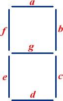
Fig. 4. 7-segment LED display
| Table 1. Inputs and outputs of the BCD to 7-segment decoder | ||||||||||
| D3 | D2 | D1 | D0 | a | b | c | d | e | f | g |
| 0 | 0 | 0 | 0 | 0 | 0 | 0 | 0 | 0 | 0 | 1 |
| 0 | 0 | 0 | 1 | 1 | 0 | 0 | 1 | 1 | 1 | 1 |
| 0 | 0 | 1 | 0 | 0 | 0 | 1 | 0 | 0 | 1 | 0 |
| 0 | 0 | 1 | 1 | 0 | 0 | 0 | 0 | 1 | 1 | 0 |
| 0 | 1 | 0 | 0 | 1 | 0 | 0 | 1 | 1 | 0 | 0 |
| 0 | 1 | 0 | 1 | 0 | 1 | 0 | 0 | 1 | 0 | 0 |
| 0 | 1 | 1 | 0 | 0 | 1 | 0 | 0 | 0 | 0 | 0 |
| 0 | 1 | 1 | 1 | 0 | 0 | 0 | 1 | 1 | 1 | 1 |
| 0 | 0 | 0 | 0 | 0 | 0 | 0 | 0 | 0 | 0 | 0 |
| 0 | 0 | 0 | 1 | 0 | 0 | 0 | 0 | 1 | 0 | 0 |
The design file for this example is given below. This file must have the extension .TDF.
TITLE "LED";
DESIGN IS lab1
DEVICE IS "EPM7128";
SUBDESIGN lab1
(
d0, d1, d2, d3 :INPUT;
a, b, c, d, e, f, g :OUTPUT;
)
BEGIN
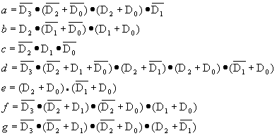
a = !d3 & (!d2 # !d0) & (d2 # d0) & !d1;
b = d2 & (!d1 # !d0) & (d1 # d0);
c = !d2 & d1 & !d0;
d = !d3 & (!d2 # d1 # !d0) & (d2 # !d1) & (d2 # d0) & (!d1 # d0);
e = (d2 # d0) & (!d1 # d0);
f = !d3 & (!d2 # d1) & (!d2 # d0) & (d1 # d0);
g = !d3 & (!d2 # d1) & (!d2 # d0) & (d2 # !d1);
END;
Once this file has been saved in ASCII format onto a diskette, you are ready to process the file. First, start MAX+PLUS II by double clicking on the MAX+PLUS II icon under Windows.
MAX+PLUS II groups files into projects. A typical project will have a dozen or more files, one or two created by the user and the rest created by MAX+PLUS II during its operation. Choose File from the main menu and select Project. Use Name to create a new project or open an existing project from the list. Once the project is active, use the File|Open or File|New option to open an existing .TDF design file or create a new one.
To ensure that you have entered the design correctly, you can check the file for syntax errors. This can be done by simply choosing Save & Check from the File|Porject. If any syntax errors are found, the Message window opens.
After locating and correcting all the errors, you can then compile this project. The procedure is given below:
1. Open the compiler window by choosing Compiler from the MAX+Plus II menu.
2. Select the MAX device family and the device. Choose Device from the Assign menu. The dialog box is displayed. Next, choose MAX7000S from the Devices Family. Then choose AUTO or EPM7128SLC84-7 from Devices. Click OK.
3. Choose the Start button to begin compiling.
When the Compiler finds errors, a Message window is shown below the compiler window. You can use it to locate the errors in the .TDF file. After you correct these errors, you must recompile the project.
Once the file has been compiled correctly, you can simulate your design before programming the EPM7128 chip. To do this, create a vector file (with the extension .VEC) and save it as an ASCII file. A sample file for this design is shown below. Note that all inputs and outputs in the .VEC file must also be in the .TDF file, but the reverse is not necessarily true.
UNIT ns;
START 0;
STOP 550ns;
%THE UNIT (ns) IS APPLIED HERE%
INTERVAL 50;
INPUTS d3 d2 d1 d0;
OUTPUTS a b c d e f g;
PATTERN
%START OF VECTORS %
% d3 d2 d1 d0 %
0> 0 0 0 0
50> 0 0 0 1
100> 0 0 1 0
150> 0 0 1 1
200> 0 1 0 0
250> 0 1 0 1
300> 0 1 1 0
350> 0 1 1 1
400> 1 0 0 0
450> 1 0 0 1 ;
% end of vectors%
To begin a simulation session, specify the source of the input vectors for simulation and create Log and History files that record the simulation session. To open the simulator and specify inputs and outputs:
1. Choose Simulator from the MAX+PLUS II menu. The simulator window opens.
2. Choose Inputs/Outputs from the File menu. A dialog box is displayed.
3. In the Input (.scf or .vec) field, specify the source of input as the .VEC file. The output file is converted automatically to an equivalent .SCF file.
4. Select the History (.HST) and Log (.LOG) options.
5. Choose OK.
To simulate the design, choose the Start button. When the simulation has finished, the simulator lists overall results in a message box. In addition, the waveforms of the inputs and corresponding outputs are recorded in the .SCF file. You can check this file by choosing the Open SCF button.
The last step is to create a table file which is an ASCII alternative to the output in the .SCF file. To create a table file:
1. Choose Create Table File from the File menu.
2. Type a name in the File Name box and choose OK. The .TBL extension is appended automatically.
Table files can be viewed with the MAX+PLUS II text editor. The table file for our input vector file is shown below.
%
INPUTS d3 d2 d1 d0 ;
OUTPUTS a b c d e f g ;
UNIT ns ;
RADIX HEX ;
PATTERN
% d d d d %
% 3 2 1 0 a b c d e f g %
0.0> 0 0 0 0 = 0 0 0 0 0 0 1
50.0> 0 0 0 1 = 0 0 0 0 0 0 1
57.5> 0 0 0 1 = 1 0 0 1 1 1 1
100.0> 0 0 1 0 = 1 0 0 1 1 1 1
107.5> 0 0 1 0 = 0 0 1 0 0 1 0
150.0> 0 0 1 1 = 0 0 1 0 0 1 0
157.5> 0 0 1 1 = 0 0 0 0 1 1 0
200.0> 0 1 0 0 = 0 0 0 0 1 1 0
207.5> 0 1 0 0 = 1 0 0 1 1 0 0
250.0> 0 1 0 1 = 1 0 0 1 1 0 0
257.5> 0 1 0 1 = 0 1 0 0 1 0 0
300.0> 0 1 1 0 = 0 1 0 0 1 0 0
307.5> 0 1 1 0 = 0 1 0 0 0 0 0
350.0> 0 1 1 1 = 0 1 0 0 0 0 0
357.5> 0 1 1 1 = 0 0 0 1 1 1 1
400.0> 1 0 0 0 = 0 0 0 1 1 1 1
407.5> 1 0 0 0 = 0 0 0 0 0 0 0
450.0> 1 0 0 1 = 0 0 0 0 0 0 0
457.5> 1 0 0 1 = 0 0 0 0 1 0 0
550.0> X X X X = X X X X X X X
;
Once you have reviewed the .TBL file and you are satisfied with your design, you are ready to assign input/output pins and program the device.
The pin assignment for the LED on the UP1 Education board are specified below:
|
Dislay segment |
Pin for Digit 1 |
Pin for Digit 2 |
| a | 58 | 69 |
| b | 60 | 70 |
| c | 61 | 73 |
| d | 63 | 74 |
| e | 64 | 76 |
| f | 65 | 75 |
| g | 67 | 77 |
| Decimal Point | 68 | 79 |
To assign an input/output pin, choose Pin/Location/Chip from the Assign menu. Click Assign Device and select EPM7128SLC84-7 and click OK. Then enter the variable name in the Node Name field, (for example, a), choose Pin in Chip Resource and enter the pin number (for example, 58) and then click the Add button. Repeat until all input/output variables are assigned. You need to recompile after assigning the input/output pins.
To program a device:
1. Choose Programmer from the MAX+plus II menu.
2. Click on the Program button.
The Programmer examines the device (each device is automatically blank-checked before it is programmed), programs the current programming file into the device, and verifies the newly programmed contents of the device against the original programming file. If the Auto-Testing command is turned on, the programmer also functionally tests the programmed device with the input vectors in the current .SCF file, vector file, or programming file.
4. A Sequential Example: A Dice Tosser
The example of the dice tosser which will be presented is based on a design which appeared in the “PAL Programmable Array Logic Handbook,” Third Edition, 1983, Monolithic Memories Inc. (MMI), Santa Clara, CA 95050. It is desired to design a ``dice tosser" with the EPM7128S.
Table 2 shown the state transition diagram for the dice to display 1 to 6 on the LEDs.
| Table 2. The state transition table of one die. | ||||||
|
Die Toss |
Present State | Next State | ||||
| Q3 | Q2 | Q1 | D3 | D2 | D1 | |
| 1 | 0 | 0 | 1 | 0 | 1 | 0 |
| 2 | 0 | 1 | 0 | 0 | 1 | 1 |
| 3 | 0 | 1 | 1 | 1 | 0 | 0 |
| 4 | 1 | 0 | 0 | 1 | 0 | 1 |
| 5 | 1 | 0 | 1 | 1 | 1 | 0 |
| 6 | 1 | 1 | 0 | 0 | 0 | 1 |
The output Q’s are in term decoder by a BCD to LED decoder as describe in the first part of this laboratory.The equation for the first die is
The same procedure used for the second die produces essentially identical state equations:

The design file for this example is given below. In this file, D[6..1] defines the six D flip flops. Their inputs are D6.d--D1.d, and their outputs are D6.q--D1.q. Q[6..1] is the outputs of the chip.
TITLE "DICE";
DESIGN IS dice
DEVICE IS "EPM7128S";
SUBDESIGN dice
(
clk : input;
Q[6..1] : output;
)
VARIABLE
D[6..1] : dff;
BEGIN
D[].clk = clk;
D1.d = (D2.q & !D1.q) # (D3.q & !D1.q);
D2.d = (!D2.q & D1.q) # (!D3.q & !D1.q);
D3.d = (D3.q & !D2.q) # (D2.q & D1.q);
D4.d = (D5.q & !D4.q) # (D6.q & !D4.q);
D5.d = (!D5.q & D4.q) # (!D6.q & !D4.q);
D6.d = (D6.q & !D5.q) # (D5.q & D4.q);
Q[] = D[].q;
END;
Once the .TDF file is created, you should follow the same compile-simulate-program procedure as used in the previous design. There is one important part that has been excluded from the previous example: how to handle unassigned states. Under certain circumstances, particularly on power-up, it is possible for the circuit to enter an unassigned state. It may eventually get to a known state on its own, or it may cycle among the unassigned states forever. To handle this, a good design should force a transition from each unassigned state to a known state; these transitions should be incorporated into the state equations.
5. Lab Assignments
1. Program the EPM7128S to realize the 7-segment decoder. Use MAX+PLUS' built-in simulation to verify the design.
2. Program the EPM7128S to realize the dice thrower. Use the 7-segment to display the value of the dice.
6. Pre-lab assignments
Review Chapter 6, pp. 202--217 of Computer Engineering Hardware Design. by M. Morris Mano. Students should obtain their unique dice sequences from the lab instructor. The student should prepare designs similar to those presented in this experiment which will realize the required functions. Note that the 7-segment is illuminated by driving the I/O pin with a logic zero. For the sequential design, the students should include transitions from each unassigned state to the first state in their sequences.
7. Equipment and parts needed
• One Altera University Program Design Laboratory Package.
8. Refereneces
1. Computer Engineering Hardware Design by M. Morris Mano, Prentice Hall, 1988.
2. MAX+PLUS II Users Guide, Altera Corp., Santa Clara, CA, 1991.
|
Go to COE394 Experiment | 1 | 2 | 3 | 5 | 6 | 7 | 8 | 9 | ECE Lab home |
|