Go to EE392 Experiment | 1 | 2 | 4 | 5 | 6 | 7 | 8 | ECE Lab home
![]()
|
|
Go to EE392 Experiment | 1 | 2 | 4 | 5 | 6 | 7 | 8 | ECE Lab home |
|
EXPERIMENT III
COMMON EMITTER AMPLIFIER
OBJECTIVES
Experience in design of a single stage amplifier. Simulation of circuit performance with PSPICE and comparison with measured values.
PRELAB
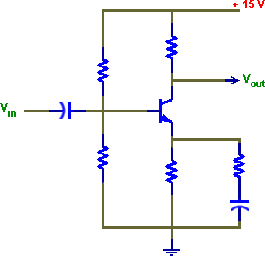
Design a common emitter amplifier following the schematic shown in the figure below (see ref. 1).
Design requirements:
Gain at quiescent point between 40 and 100, specified by the instructor for each group;
f-3dB must be not larger than 200 Hz;
Vcc = 15 volts;
Quiescent current Ic = 0.5 mA.
Specify component values to meet these requirements but check also the parts selection in your kit. Obtain components from other sources, if needed. You may deviate from the design specification by 10% if you do not find the required components.

Check your design by simulating circuit performance with PSPICE using the same signals as you will use in the laboratory.
References:
T. C. Hayes and P. Horowitz "Student Manual for The Art of Electronics" Cambridge University Press 1989, pp. 115 - 117
P. Horowitz and W. Hill "The Art of Electronics" 2nd ed. Pp. 82 -85.
LABORATORY
1.
ASSEMBLY AND
TESTING
Wire the amplifier circuit following your design. Measure VE, VB, and VC in quiescent conditions. Drive the input with small sinusoidal signal (output should not exceed 1 V) and measure the values of the design parameters: small signal voltage gain, quiescent current, and the frequency f-3dB. Use DVM for accuracy but note the phase relation between input and output waveforms.
Measure also input and output impedances. To find input impedance, connect a series resistor to the input and measure voltage across it. To find output impedance, load the output with a resistor (through a capacitor!) and measure output voltage drop due to the load.
Note: Circuits with high gain may oscillate. To prevent this, make neat and short connections between components and pay attention to grounding. Fixed resistors and capacitors are preferred to resistance and capacitance boxes.
2. FINE TUNING
If the measurements do not agree with the design parameters, fine tune your circuit by replacing or adding resistors. You may also introduce a trimming (adjustable) resistor for convenient tuning. Do not be concerned with obtaining an exact value of f-3dB as long as it is not larger than specified.
REPORT
In the report compare the design parameters with their measured values. Describe any fine tuning which had to be done on the circuit. Compare measurements with simulation results from PSPICE, including the measured f-3dB vs. the value from simulated frequency distribution of the circuit. Compare measured and calculated values of input and output impedances.
To improve this amplifier you could expand this circuit by adding more stages (transistors).
What would you do to:
Increase the
input impedance
Decrease the output impedance
|
|
Go to EE392 Experiment | 1 | 2 | 4 | 5 | 6 | 7 | 8 | ECE Lab home |
|