Go to ECE392 Experiment | 1 | 2 | 3 | 4 | 5 | 6 | 8 | Lab manuals | ECE Lab home
![]()
|
|
Go to ECE392 Experiment | 1 | 2 | 3 | 4 | 5 | 6 | 8 | Lab manuals | ECE Lab home |
|
ECE 392 - Electrical Engineering Laboratory II
EXPERIMENT VII
DIGITAL CIRCUITS
OBJECTIVES
Introduction to digital circuits. TTL and CMOS digital integrated circuits. Basic gates and flip-flop circuits.
INTRODUCTION
Digital circuits represent great majority of integrated circuits manufactured today. Among them MOS and CMOS devices are most prevalent but TTL circuits based on bipolar device technology are still important. Although both types of devices may perform identical logic functions their behavior and signal or power requirements are somewhat different. It is a good idea to acquaint yourself with these differences from the start. Properly treated digital circuits will reward you with predictable and reliable performance allowing you to concentrate on the logic problem at hand.
We will experiment with two different digital devices: logic gates and sequential circuits, so called flip-flops. While the output of a logic gate is completely determined by its input states, the output of a flip-flop depends also on the past states, i.e. the device has elementary memory. . Flip-flops are basic building blocks of counters, arithmetic accumulators, and other important circuits. Flip-flops are combinations of logic gates and are controlled not only by input signals but also by clock pulses. The latter feature ensures that the output states change only at a certain time, synchronously with a system clock which controls many devices in a complex circuit.
For consistency we
will power all digital circuits with a single polarity power supply providing
standard voltage +5 V with respect to ground. Input states can be realized with
switches providing connections to the same power supply or to ground. In any
case do not drive inputs with voltage levels exceeding the power supply voltage.
PRELAB
Design an exclusive OR gate (XOR), using standard gates in your parts kit.
Design a digital circuit which will tell you by lighting an LED that a given month of the year has 31 days. The month is to be represented by a binary number entered by switches with positions corresponding to binary digits (0 and 1). For example, June is represented by 0110 or switches in states: off, on, on, off. You may use K-maps as an aid in the design if you wish.
Prepare also tables showing operation of D and J-K flip-flops i.e. the status of outputs for different input states.
References:
P. Horowitz and W. Hill The Art of Electronics, Cambridge University Press 1989, 2nd edition, parts of chapters 8 and 9.
T. C. Hayes and P. Horowitz "Student Manual for The Art of Electronics", pp.309-339.
LABORATORY
Equipment needed from the stockroom: scope probe, analog multi-meter, resistance substitution box, leads.
1. SIMPLE DIODE GATES
You can easily assemble basic logic gates using diodes and resistors:
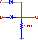 |
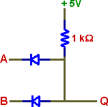 |
| (a) | (b) |
Assemble and test the two circuits shown above. What logic functions do they perform? What are disadvantages of these simple circuits that make them unsuitable for a wide use in digital systems?
2. INTEGRATED CIRCUITS GATES
|
|
|
|
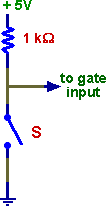
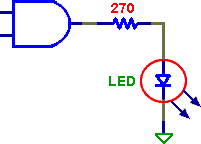
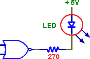
| Defining input states with a switch and indicating output states with an LED. | ||
2.1 Output Voltage Levels
Examine two integrated circuit gates in your parts kit, one TTL and one CMOS. Use 5 V to supply the chips and switches for setting input states, as shown above. Check the logic functions they perform (the truth table).
Note the HIGH and LOW output voltage levels for both types of chips.
2.2 Threshold Input Voltage
With one gate input set to HIGH vary the voltage at the other input and note the level at which the gate output switches states from H to L and from L to H. Make this threshold voltage measurements for both TTL and CMOS devices. Do not apply to the inputs higher voltage than the supply voltage of the chip! To be safe use a 10k potentiometer connected between the power supply (+5 V) and ground. Center tap of the potentiometer will give you adjustable voltage for the gates input.
2.3 Floating Inputs and Undefined States.
In TTL gate, disconnect the inputs and examine the output state. Measure voltages on the inputs with DVM. What states are assumed by floating inputs in TTL devices? What needs to be done to assert these inputs LOW?
In CMOS gate connect one input to HIGH and leave the other undefined by attaching to it a few inches length of wire. Observe output while moving your hand over the wire.
CMOS circuits draw practically no power when left in a given state (quiescent operation) They have two complementary transistors in series between power source and ground with one of the transistors in the "off" state. These circuits, however, draw current during switching which transfers charge to the gate capacitance. To examine a serious problem which occurs when CMOS input states re undefined, connect all input gates on a chip to the center tap of a 10k potentiometer connected between power supply and ground. Place an analog ammeter between the chip supply pin and the power supply. There should be only a small supply current when the gate voltage is HIGH or LOW. Switch the ammeter range to 100 mA, or more, and observe the supply current as you turn the potentiometer so that the gate input state becomes undefined. When you see the current surge change the state to L or H or turn off supply voltage. Leaving the circuit with high supply current can overheat it and damage.
These experiments should demonstrate to you important practical rules of digital circuits:
All input states should be well defined, either LOW or HIGH.
These levels should be in appropriate voltage range for a given device type.
Never leave inputs floating. Tie unused inputs to the power source or ground.
These rules are especially important for CMOS devices, the most popular today. By following them you will avoid a lot of problems in your practice.
3. COMBINATIONAL LOGIC WITH GATES.
Build an exclusive OR gate (XOR) with chips available in your parts kit.
Demonstrate a digital circuit indicating which month of the year has 31 days (see Prelab).
4. SEQUENTIAL CIRCUITS (FLIP-FLOPS).
4.1 D and J-K Flip-Flops
Examine operation of both D and J-K flip-flops by asserting different input states using switches. Use square wave from the waveform generator as a clock signal. Use proper DC bias in the generator to obtain positive pulses. Prepare tables showing input and output states.
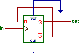
Using D flip-flop, verify that the timing of the state change is defined by the edge of the clock pulse. To do this, connect Q to D and watch the clock and D signals on the scope. Increase the clock frequency and observe propagation delay or the delay between the edges of the clock and Q pulses.
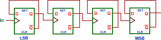
A circuit for testing timing of a D flip-flop and a four digit binary ripple counter.
4.2 Ripple Counter
You noticed in the previous circuit that the frequency at Q was half of that at the clock input. The circuit effectively divides the number of pulses by two. Cascading a number of such circuits one can divide the number of pulses by 4, 8,..and so on. Driving an LED with each consecutive output should give you a binary display of the number of pulses that came to the input. Assemble such a counter with four D flip-flops. Count pulses generated by a switch.
Note: Some integrated circuits contain a number of flip-flops, which can not be connected the way shown in the figure above because their clock inputs are tied together and connected to one pin. For example 74LS174 with six flip-flops has one common clock signal pin. You need four of such chips to build the ripple counter, using only one flip-flop from each chip.
In testing the ripple counter you are likely to see that the counter display does not correspond to the number of switching. This is due to the so called switch bounce - each switch closure generates not one but a number of pulses as the metal contacts come together. A remedy is a switch debouncer, a circuit easily built with logic gates which generates one pulse for each switch closure (see ref. 2). To check that your counter works properly, use a very low frequency square wave as the input to your circuit. Use proper DC bias in the generator to obtain positive pulses.
Increase square wave frequency to observe ripple effect or time lag between pulses coming from different segments. This undesirable delay can be eliminated in synchronous counters built with K-J flip-flops in which all pulses are synchronized with the clock signal.
REPORT
Present all schematics and measurements. Include tables showing input and output states of gates and flip-flops. Include observations on the circuits performance and provide explanations.
|
|
Go to ECE392 Experiment | 1 | 2 | 3 | 4 | 5 | 6 | 8 | Lab manuals | ECE Lab home |
|