This
document contains a step-by-step tutorial for generating the layout of an
inverter in the Mentor Graphics application IC Station. It covers
opening IC station and creating a cell, generating layout, and checking
the design for errors (DRC and LVS). Documents covering extracting
parameters for analog simulation and advanced tip for editing cell layouts
are also linked below. Separate documents began and continue the
tutorial for other Mentor applications.
General
Information
Opening
IC
Generating
Layout
Checking
your Layout
Parameter
Extraction
Calibre_PEX: Extraction of Parasitic
Capacitance and Resistances for HSPICE Simulation
Editing
Cell Layout
At this time, you should have
completed schematic entry in DA and functional simulation in
Accusim or Hspice. You should also have created the design viewpoint for your
inverter cell. You should also be familiar with the mask layers and
design rules which are covered in text for this course.
Note, throughout this tutorial we
have used both L and l
to represent the minimum feature
size lambda.
Preparing the design
for IC station:
The
adk_dve script that you ran for simulation also creates the viewpoints needed
for layout and verification. You only have to do this once per design.
Even if you make changes to your design you don't have to do this again.
If you do, the script will do nothing and that's OK. If you
decide to change the technology, however, you must rerun the script with
the appropriate technology parameter.
Opening IC station:
Make sure you are
in your working directory and have typed the 'swd' command. Then, at
the command prompt, enter
>
mentor.2002 adk_ic
&
Setting
Up IC Station: 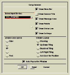
Maximize the IC
Station window so you have lots of room to work on your layout, and setup
your environment by selecting the following from the main
menu
MGC > Setup > Session
and selecting
Up Down Tiling. Leave everything
else as default and click 'OK'.
Creating your Cell
From the main Session
Palette on the right, select
Create (under
heading of Cell)
or alternatively, using the main menu,
select
File >
Cell > Create
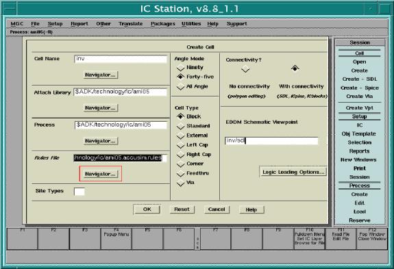
The figure below
shows the window that should pop up. In the Cell Name space, enter the name of the cell as
inv.
Click on the Navigator button under Attach
Library then click on the 4-direction arrows and enter the
directory
$ADK/technology/ic
then click 'OK' to view all available
libraries. Select 'tsmc035' (choose the
icon with the 'L' symbol, not the folder symbol) and click
'OK'.
Follow the same
procedure for Process and select 'tsmc035' (choose the file with the 'P' icon, not the
folder icon).
Follow the same
procedure for the Rules File, and select the file
'tsmc035.rules'
Returning to the
Create Cell window, keep the default Angle Mode and Cell
Type, but under Connectivity select
'With connectivity'.
Enter the EDDM Schematic
Viewpoint as
inv/sdl
Finally, click 'OK' in the Create Cell window to create your
inverter cell
Back to
Top
When
your cell opens (at first, it will be a blank layout sheet), notice the
main IC
palette on the right. You will use this to access many of the IC
functions.
1. Opening
Schematic
For reference,
you might want your schematic opened so you know what circuit you should
be generating layout for. It's pretty simple for the inverter, but
here's how so you'll know for more difficult cells. To open your
schematic, go to the IC Palette and
select
DLA Layout > Open
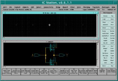
Your schematic
should appear below your layout window provided you set up
the tiling as instructed above. From the DLA Layout palette, click
Top to return to the main IC
Palette.
2.
Beginning Transistor Layout:
Before actually starting
the layout, you need to know more about the grid of your layout
window. From the main menu, select
View > Zoom
> To Grid
Your layout window will now show the
smallest grid point to which you can align your layer polygons. The
spacing between two immediate dots in the grid is 0.5L or 0.5l
(i.e., 2
grid points equals 1l).
Use this grid to help determine the size of each polygon you draw.
Also notice near the center of this window you will see a large white
+ symbol. This represents the
origin of the cell and is the 0,0 point for the position cursor which is
constantly updated just above your layout window and below the main menu
bar. Typically we want to set the origin of each cell to the lower
left corner. More discussion on cell origin is provided later in the
tutorial.
3.
Adding Shapes
From the main IC
Palette, select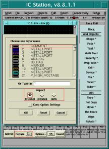
Easy Edit >
Shape
This will open a dialog box at the bottom of the
screen titled 'ADD SH'. Click on the Options tab to view and select the layers you will
need to draw your transistors.
You can
either select a layer by clicking on it or you can type the name of the
layer in the Or Type In box. Click
the 'Keep Option Settings' button if you want
this layer to be the default layer (i.e., it will automatically be
selected each time you use the Add Shape command). Use the scroll
bar to move down to layer 43, ACTIVE.
Select this layer and click
OK.
Scroll
down the list to find the layer you want. Start by choose the active layer. Click on
active and then click OK. The mouse
pointer changes to + format. In the
layout cell window, click and drag to form a
rectangle that is 15L (width) x 5L (height). At this point the
polygon is selected and will appear as an unfilled rectangle. Press F2 to unselect the object and it will fill with
the pattern for that layer.
The
function keys, in combination with shift/control/alt, provide you with
many commands that you will use often. These are shown at the bottom
of the IC window. Practice using the functions, Select, Unselect, Move, and Copy. When you are done, save only one ACTIVE rectangle and delete all
others.
4.
Adding more layers:
Next, add a POLY
layer.
Draw a rectangle 2L (width) x 9L (height) (W/L=5/2) cutting midway through
the ACTIVE layer such that the top and
bottom of POLY rectangle are 2L above
and below the ACTIVE layer.
Continue
selecting new layers and adding to form the transistor. Cover the
ACTIVE layer with a N_PLUS_SELECT (which we'll call N-SELECT) layer to begin forming an nMOS
transistor (notice we do not have a N-Well layer, consistant with an nMOS
device). The N-SELECT layer should overlap the ACTIVE by 2L on all sides (determined by design
rules). The region where POLY
overlaps the ACTIVE layer
with N-SELECT forms the n-type MOS
Gate. To form a p-gate we would need an N-Well and would replace
N-Select with P-Select.
Note there are many editing functions that allow you to cut,
notch, stretch, etc. any polygon you draw. You will need to become
familiar with many of these functions. More information on these is
provided in a supplement document Editing
Cell Layout. If you practice these functions, make sure you have
only the layers specified above when you return to this part of the
tutorial.
To form
a substrate tap, you will need a
combination of the layers ACTIVE and
P-SELECT. Add
a tap now. Later we will want to form an n-well tap, which will need a combination of
ACTIVE and N-SELECT inside an N-WELL layer. These taps are also called
pdiff and ndiff.
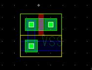 For this
tutorial, right now you should be trying to build a single nMOS transistor
with associated substrate tap. It should look like the figure to the
right, except without contacts and metal which will be added later.
Make your layout look like the figure before moving on.
At
this point, let's save the cell so we don't lose any work incase of
computer crash or other acts of God. Select
File > Cell
> Save Cell > Current Context
Before we can continue, we need to
reserve our cell. Every time we save the cell, it will no longer be
reserved for edit. So, if you want to modify your cell (and you
do!), select
File > Cell > Reserve > Current context.
5.
Checking the layout:
Once you have the basic layers for your
transistor, you should check to make sure you have not violated any design
rules. You should do this frequently so that you can correct errors
as they occur rather than waiting until you are done when you might have
many errors to correct. Jump to Design
Rules Checker then come back here and continue.
Note: This first time through the DRC check, you will get
one or more 'bad_contact' (or similar) errors. Ignore these for now;
you will fix them in the next step.
6.Making contacts:
Now we
need to create electrical connections from the active regions to
upper-level metal layers which we will do using contact layers. We will be using two
different contact layers, one for contact to the active region, CONTACT_TO_ACTIVE, and one for contact between
metal1 and poly, CONTACT_TO_POLY.
To simplify, we will use the terms ACONT
and PCONT, respectively, as given in the
DRC Document.
Consider
first the nMOS transistor. Since this is an n-well CMOS process, the
nMOS transistors must be formed in the p-substrate with an associated
substrate contact called a tap. The
substrate will be connected to the ground or VSS of the circuit. The
source of the nMOS transistor will also be
connected to ground, and the drain of the
transistor will (eventually) be connected to the output node.
Using the
ACONT
(CONTACT_TO_ACTIVE) layer,
add contacts to the source and drain following the Adding Shapes step above. Next add a
contact to the tap active layer. Then, add a METAL1 layer across the bottom of your
transistor, covering the tap contact and stretching across the full width
(left-to-right) of the P-SELECT layer.
This will form the ground power supply rail in your design (discussed more
in the note below). You should make the METAL1 ground
rail as wide as the tap active layer (5L). Although this is larger
than the minimum size of metal1, we want the ground (and VDD) rails to be
able to handle more current and therefore be wider than minimum
size.
Finally,
you need to connect the source of the
transistor to the ground rail using
METAL1.
You can either add a new polygon to connect the source contact (left side
of the transistor) to the tap contact, or you can try the notch
command to modify the metal1 power rail polygon. Either way, make
sure your source and substrate tap are connected.
When you
are done, your cell should look very similar to the figure
above. Save your cell and then reserve it for edit before
continuing.
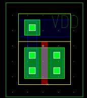 7.
Do it All Again
Repeat the processes above to form a pMOS
transistor with a tap to the n-well. Your pMOS transistor should
have W/L = 10L/2L to match your schematic (you will need to draw the
active layer 15L x 10L). You will, of course, also have to add the
N-WELL layer which should surround your
transistor and tap active layers according to the design rules. Once
you have added all of the shapes, your pMOS should look like the figure to
the right.
Note about cell pitch. In
large-scale VLSI design (i.e., with many transistors/gates/cells), it is
important to make the cell layouts have uniform height so that they will
match when placed side-by-side. Typically, we will design each gate
with a VDD rail at the top and a Ground rail at the bottom. If we
place two cells together, we want these power rails to match-up.
This will make more sense when we start putting together several gates
later in the course. We define pitch as the
distance from top to bottom of our layout cell, measured from the
top if the VDD rail to the bottom of the Ground rail. For this
course, we will use a cell pitch of
50l.
Some larger cells might not match this size, but all the basic logic gates
should have a layout height of 50l.
8.
Final Layout Steps
Finally, the layout of the inverter can be
obtained by stacking the two transistors and connecting them as
required. Connect the drains using METAL1 to form the output. Join the
POLY of the two gates to form the input
by adding another polygon or modifying one of the existing
polys.
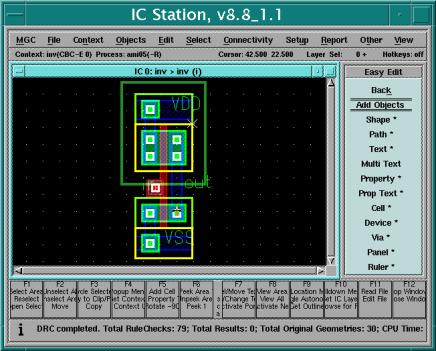
Since we
often want to connect to the input gates from metal1, you should add a
metal1 contact to poly on your input. Notch your POLY input near the middle of the cell to be
at least 5Lx5L, add METAL1 on top of
this, then add PCONT (CONTACT_TO_POLY)
in the
center of these shapes. The final layout should be very similar to
that shown below.
Once you
think you have the layout complete, you should check
for DRC errors and fix them before continuing. Jump to Design
Rules Checker then come back here and continue.
9.
Adding the ports
In order for the software tools to
match your layout to a schematic, we need to assign a few port values to
our input and output nodes. The first step is to make sure you have
deselected everything by pressing F2. Then select the layer to be
made a port. For this example, we want to make the metal1
layer that connects the two drains into an output
port, and the metal1 layer that is connected to the gate poly to be
an input port. Do these one-at-a-time,
and be sure to unselect one before selecting the other.
With the desired
layer selected, to make the port, use the main menu to select
Connectivity
> Port > Make port
In the prompt bar, enter the
following into the dialog boxes (use TAB to move between
fields)
For an input port,

Port Type =
Signal; Direction = in; Port Name = in, then click OK. (Use
in rather than in1 which is shown in the
figure).
Repeat for the
output port (unselect the input first!) setting
Port Type = Signal;
Direction = out; Port Name = out, then click OK
We also need to
make ports of our power and ground rails. To make the VDD power port, select metal1 layer across the top of
your cell and go to
Objects
> Make > Port
and
enter the following:
Port Type = Power; Direction = In;
Port Name = VDD,
then hit return.
Repeat for the
ground power port selecting the metal1 layer at
the bottom of your cell and naming it ground.
Finally, unselect
all everything by hitting the F2 key.
10. Adding
Property Text
Following steps similar to adding ports, add Property
Text to the input, output, and power ports. Select one port at a
time and the select
Easy Edit >
Property Text
to add text to your layout. Use the same
names as you used for the ports, in, out, VDD,
ground. You can vary the set the size of the text by clicking
on the Options tab and entering a value in units of 'grids'. 5 is
recommended. You should keep the default layer setting -don't change
this, even if you like other colors better =).
11. Setting
the cell origin:
When we instantiate
cells into higher-level layouts, we need to have a reference point for the
cell. This is the 'cell origin'. To make life easier, it is
recommended that you set the origin of all cells to the same general
location. From the main menu, select
Context > Set
cell origin
The mouse pointer changes to + form and you must click on the spot where the
origin is desired. Set the origin of your inverter to be the bottom
left-hand corner of the ground rail metal1 layer (where it meets the
p-select layer placed around the substrate tap).
Very Important: Once you
instantiate a layout cell into a higher-level cell, you should NOT change
the origin as this will cause the cell to shift within the higher-level
cell disrupting any connections you would have made.
Back to
Top
During this
tutorial, you will be asked to jump down to this section and complete a
few step before going back to continue above. However, after you
complete the previous section, you should go through the DCR check one
more time and then complete the LVS steps outlined below before continuing
to the Extraction section.
Design Rule Checker
From the
main menu, select
Checking >
DRC (IC rules)
to began
a rules check. The number of DRC errors will appear
at the bottom of the screen as total results. A description of
the errors can be obtained by selecting
Checking >
First Error
then,
after the first error, select
Checking >
Next Error
For each
error, the area under violation is highlighted and described at the bottom
of the screen. Correct errors by moving/editing layers and
conforming to the DRC rules. Contiue corrections and DRC checking
until you have no rules violations.
To go back
to the Generating Layout part of the tutorial, click
here.
LVS( Layout Vs Schematic):
The
LVS process compares the layout with the schematic to verify your
layout matches. In the main IC Palette select
IC Trace
(M)
Then press
Load
Rules
and enter
/class/lib/564.rules
then click
OK.
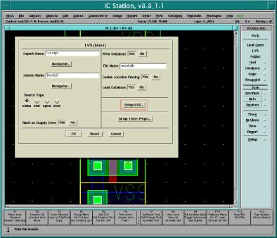 While still in the IC Trace (M) palette,
select
LVS
and enter the name of
the schematic to which you will compare your layout. Here you should
enter
inv/sdl
and set
all others to default. Click
OK.
The LVS checker will begin comparing your layout
to your schematic. When this is done, you will see that mask
results database loaded appears at the bottom of the screen.
Select
Report >
LVS
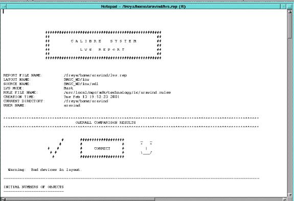
on the IC trace(M) palette. A successful LVS shows up a
smiley face with a CORRECT sign as shown in the figure below. If
there are errors, the information in this report will help you track and
fix those errors. Fixing errors will involve moving/modifying/adding
layers, checking/correcting port definitions, etc. Learning how to
track and fix LVS problems is a major part of learning these CAD
tools.
Before you
finish, you MUST PASS LVS and get a smiley
face.
Very Important: be sure to close
the LVS report before running another LVS. Otherwise, the old report
will not be overwritten and you will see the old LVS report when you open
it.

Although you must
fix all errors, you can ignore the warning about bad devices in the
layout.
Once you have
successfully passed LVS, you should save your cell.
Select
File > Cell
> Save Cell > Current Context
and you are done! Well, you're
almost done.
Back to
Top


 While still in the IC Trace (M) palette,
select