|
Go to ECE394 Experiment | 1 | 3 | 4 | 5 | 6 | 7 | 8 | 9 | Lab manuals | ECE Lab home |
|
ECE394 - Digital Systems Laboratory
Experiment 2
Combinational Circuits
1. Introduction
Logic circuits for digital systems can generally be classified into two categories. One is combinational logic circuits, the other is sequential logic circuits. A combinational logic circuit consists of logic gates whose outputs at any time are determined directly from the present combination of inputs without regard to previous inputs. In other words, the combinational logic circuits do not have the ability to memorize their past. On the other hand, a sequential logic circuit consists of not only logic gates but also memory elements. Therefore, the outputs of sequential logic circuits depend not only on the present values of the inputs but also on the input's previous values. In other words, the outputs of a sequential logic circuit are functions of its present inputs and the previous state of its memory elements. Sequential logic circuits will be the topic of your next lab.
No matter how complex a combinational logic circuit might possibly be, it will always be comprised of basic logic gates such as NAND gates, NOR gates, inverters and so on. The logic function that a combinational logic circuit represents is usually expressed using a Boolean function, or a set of Boolean functions. Quite often, the given Boolean functions to be implemented in combinational logic circuits are not simplified (minimized). In order to keep the number of the logic gates that implement the Boolean functions minimum, these Boolean functions must be simplified before they are implemented in discrete logic circuits. In VLSI design other criteria such as propagation delay and interconnect regularity may lead to designs which do not minimize total gates.
There are two ways of simplifying a Boolean function. One is to use Karnaugh map. Detailed descriptions on how to use Karnaugh map to simplify Boolean functions can be found in Chapter 2, Contemporary Logic Design† . The other method used to simplify Boolean functions is the basic laws and relations in Boolean algebra. These laws and relations are effective in simplifying Boolean functions because there is no need to have the truth tables of the functions. Some commonly used laws and relations are listed in Table 1 below.
|
Table 1 |
|
| Idempotency | X + X = X X · X = X |
| Zero and one | 0X = 0
1X = X
0 + X = X 1 + X = 1 |
| Double negation |
|
| Complementation laws |
|
| Associative laws | X + (Y + Z) = (X
+ Y) + Z = (X + Z) + Y
X(YZ) = (XY)Z = (XZ)Y |
| Distributive laws | X (Y + Z) = XY +
XZ
X + YZ = (X + Y) (X + Z) |
| Absorption | X + XY = X X(X + Y) = X |
| DeMorgan's theorem |
|
2. Objectives
Combinational logic is a very important part of digital systems. This lab is designed to enable students to design and analyze combinational logic circuits. Some basic, commonly used logic circuits, such as multiplexer (MUX), demultiplexer (DEMUX), and adder, are introduced. Students are required to use Karnaugh map and Boolean algebra techniques to simplify the given Boolean functions prior to implementing them. Students are also expected to have experience with gate delay and effect of fan-out on the speed of digital circuits.
3. Experiments
3.1. Exclusive OR
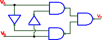
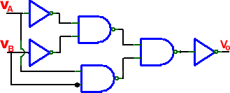
Fig. 1 shows an exclusive OR circuit. Construct this circuit using a CMOS inverter (4069) and CMOS NAND gates (4011). Verify its function by drawing the truth table. Fig. 2 shows another exclusive OR circuit. Try it out as well and verify its function using the truth table. Now derive the Boolean equations of Q in terms of its inputs A and B for both circuits, and use the relations in Boolean algebra to simplify them. Do they end up with the same XOR function?
Fig. 1. XOR. Fig. 2. Another XOR.
3.2. Half-Adder
A combinational logic circuit that performs the addition of two data bits, x and y, is called a half -adder. Addition will result in two output bits, one of which is the sum bit, S, and the other is the carry bit, C. The Boolean functions describing the half-adder are:
S = x Å y C = xy
Use the exclusive-OR circuit shown in Fig. 1 and an AND gate to build a half-adder and draw its truth table to verify its function.
3.3. Full-Adder
The half-adder does not take the carry bit from its previous stage into account. This carry bit from its previous stage is called carry-in bit. A combinational logic circuit that adds two data bits, x and y, and a carry-in bit, Cin , is called a full-adder. The Boolean functions describing the full-adder are:
S = (x Å y) Å Cin C = xy + Cin (x Å y)
Build a full-adder and draw its truth table to verify its function.
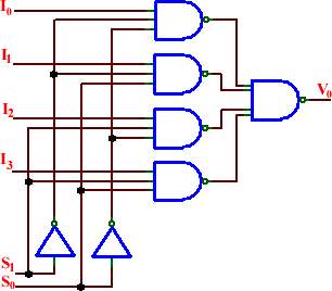
3.4. Multiplexer
Multiplexers are very useful components in digital systems. They transfer a large number of information units over a smaller number of channels, (usually one channel) under the control of selection signals. Fig. 3 is a 4-line to l-line MUX. Construct the circuit and connect the output Vo to a LED. Verify its output by setting the select signals S1 and S0, and then change the four inputs sequentially (one high, three low) to see which input signal is transferred to the output.
MUX circuits also can be used to implement random logic functions. Use a 74LS151 (8-line to l-line MUX) to design and implement a 31-day machine. The select input to the MUX is the month in binary format. The output of the circuit will be 1 whenever the month has 31 days.
3.5 Demultiplexer
Demultiplexers perform the opposite function of multiplexers. They transfer a small number of information units (usually one unit) over a larger number of channels under the control of selection signals. Fig. 4 shows a 1-line to 2-line DeMUX circuit. Construct this circuit, connect an LED to each of the outputs D0 and D1. Set the select signal S to logic 1 or logic 0, and toggle the input I between logic 1 and logic 0. Which output followed the input when S = 1 and S = 0?
 |
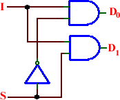 |
| Fig. 3. 4-to-1 MUX. | Fig. 4. 1-to-2 DeMUX. |
3.6. Decoder
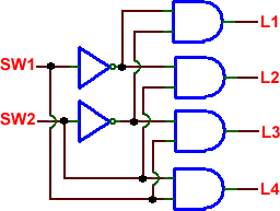
A decoder is a logic device that translates input data, which normally represents a unique input state, to a unique output that represents the input state. A good example is the decoder in memory circuits which translates binary inputs (memory addresses) to a single output to allow the CPU to access a particular memory cell specified by the input address. Use 7404 and 7408 to build a two-to-four binary decoder as shown in Fig. 5. Connect the two binary inputs A and B to two switches and the four outputs L1–L4 to four LEDs. Set the data switches to four different combinations and examine which output line will be activated for different inputs. Record the results in a truth table.
3.7. Encoder
An encoder performs a function that is the opposite of decoder. It receives one or more signals in an encoded format and output a code that can be processed by another logic circuit. One of the advantages of encoding data, or more often data addresses in computers, is that it reduces the number of required bits to represent data or addresses. For example, if a memory has 16 different locations, in order to access these 16 different locations, 16 lines (bits) are required if the addressing signals are in 1 out of n format. However, if we code the 16 different addresses into a binary format, then only 4 lines (bits) are required. Such a reduction improves the speed of information processing in digital systems.
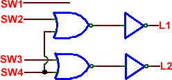
Use two NOR gates and two inverters to build a four-to-two encoder as shown in Fig. 6. The input data switch SW1 is not connected to any signal. Try to activate only one input at a time and observe the two output bits. Record the results in a truth table.
Fig. 5. 2-to-4 decoder. Fig. 6. 4-to-2 encoder.
MUX circuits also can be used to implement random logic functions. Use a 74151 (8-line to l-line MUX) to design and implement a 31-day machine. The select input to the MUX is the month in binary format. The output of the circuit will be 1 whenever the month has 31 days.
4. Equipment and parts required.
Protoboard
One CMOS Inverter (4069)
Two CMOS NAND (4011)
One CMOS NOR (4001)
One TTL NOR (7402)
One TTL Inverter (7404)
One TTL AND (7408)
One TTL XOR (7486)
One TTL NAND (7400)
One TTL 3-input NAND (7410)
One TTL 4-input NAND (7420)
One TTL 8x1 MUX (74LS151)
† Randy H. Katz, Contemporary Logic Design, The Benjamin/Cummings Publishing Co., 1994