|
Go to ECE394 Experiment | 1 | 2 | 4 | 5 | 6 | 7 | 8 | 9 | Lab manuals | ECE Lab home |
|
ECE394 - Digital Systems Laboratory
Experiment 3
Sequential Circuits
1. Introduction
In the last experiment, the logic circuits introduced were combinational. These circuits do not have memory cells and their output depends only upon the current value of the input. Memory cells are very important in digital systems. Their usage in digital circuits provides temporary storage of the outputs produced by a combinational logic circuit for use at a later time in the operation of a digital system.
Logic circuits that incorporate memory cells are called sequential logic circuits; their output depends not only upon the present value of the input but also upon the previous values. Sequential logic circuits often require a timing generator (a clock) for their operation.
The latch (flip-flop) is a basic bi-stable memory element widely used in sequential logic circuits. Usually there are two outputs, Q and its complementary value. They are called state variables. State variables which change only between logic 1 and logic 0 are called binary state variables. There are various types of latches. Some of the most widely used latches are listed below.
S-R FIip-Flop:
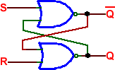
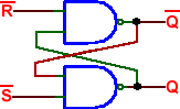
An S-R latch consists of two cross-coupled NOR gates and possibly two inverters, as shown in Fig. 1. An S-R flip-flop can also be design using cross-coupled NAND gates as shown in Fig. 2. Table 1 shows the truth tables for both cases. Note that a negative logic signal such as
is considered asserted (logical 1) when low.
Fig. 1. S-R latch with NOR gates. Fig. 2. S-R latch with NAND gates.
Table 1. Truth table for S-R latch S-R Latch NOR gates S-R Latch NAND gate R S Q Q L L NC NC L L H L L H H H L H L L H L L L H L H H H H L H H H NC NC NC- no change Clocked (Enabled) S-R Flip-Flop:
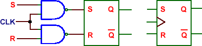
As shown in Fig. 3, a clocked S-R flip-flop has an additional clock input so that the S and R inputs are active only when the clock is high. When the clock goes low, the state of flip-flop is latched and cannot change until the clock goes high again. Therefore, the clocked S-R flip-flop is also called “enabled” S-R flip-flop.
D Flip-Flop:
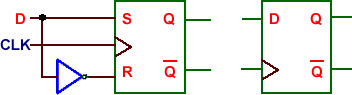
A D latch combines the S and R inputs of an S-R latch into one input by adding an inverter, as indicated in Fig. 4. When the clock is high, the output follows the D input, and when the clock goes low, the state is latched.
Fig. 3. Clocked S-R flip-flop. Fig. 4. D flip-flop. D Edge-Triggered Flip-Flop:
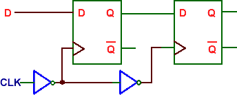
An edge-triggered D flip-flop combines two D latches, as shown in Fig. 5. The input latch is called the master and follows the input while the clock is low. When the clock goes high, the master is latched and its output is transferred to the second latch, called the slave. The slave output is seen by the user. Hence the edge-triggered D flip-flop senses the input data present at the rising edge of the clock and provides a corresponding output. The output can only change at the rising clock edge. The small triangle on the “CLK” terminal on the symbol represents its edge-triggering.
Fig. 5. D Edge triggered flip-flop.
J-K Master/Slave Flip-Flop:
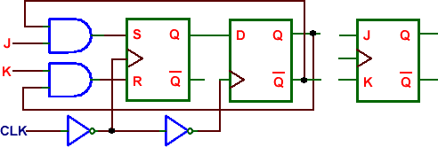
As shown in Fig. 6, a J-K master/slave flip-flop is similar to an edge-triggered D flip-flop except that J and K inputs are provided for the master. Although the output can change only at the rising clock edge, a J-K master/slave flip-flop is not truly edge-triggered because the output does not always reflect the inputs present at the triggering edge. Table 2 shows the truth table for the J-K master/slave flip-flop.
Fig. 6. J-K master/slave flip-flop
Table 2. Truth table for J-K flip-flop J K Q Operation L L q No Change L H L Reset H L H Set H H Toggle
J-K Edge-Triggered Flip-Flop:
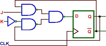
Fig. 7 shows one way of implementing a true J-K edge-triggered flip-flop, which produces an output that depends only upon the input data present at the rising edge of the clock. Unlike combinational logic circuits, sequential logic circuits present some special issues.
Fig. 7. J-K edge triggered flip-flop .
Race Condition:
If both inputs to the S-R flip-flop in Fig. 1 are changed from logic 1 to logic 0 at the same time, its outputs will be unpredictable and we call that a race condition. In logic circuit design, this condition should be avoided by making sure that 1's are not applied to both inputs simultaneously.
Set-up Time:
Set-up time for flip-flops is defined as the time interval during which a signal must be applied and maintained at a specific input terminal before an active transition occurs at the clock input. For example, set-up time for a D flip-flop is defined as the time required for the data to be present (above, or below, a threshold value) on the input before the clock transition (edge) occurs.
2. Objectives
This lab introduces the concept of sequential logic circuits and their basic working mechanisms. Students are expected to understand basic sequential circuits and the ways to measure delay time and set-up time of sequential logic circuits.
3. Experiments
3.1 Flip-Flops
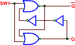
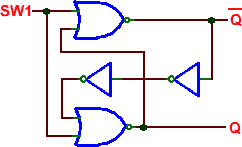
Build an S-R flip-flop using NOR gates. Check its truth table against Table 1. Now modify the S-R flip-flop according to Fig. 8. Connect data switch SW1 to a pulse generator. Observe the output, especially when input changes from 1 to 0. Now modify the circuit again according to Fig. 9 and repeat the process. What happened to the output this time? This test is actually setup to demonstration race condition. Can you explain what race condition is?
Fig. 8. S-R flip-flop Fig. 9. S-R flip-flop.
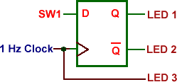
Connect a 7474 edge-triggered D flip-flop as shown in Fig. 10. Set the data switch SW1 to logic 0 and then logic 1. Observe that data transfer to the output occurs only on the positive clock edge.
Now modify the above circuit by connecting the CLK pin to SW1 instead of a clock signal. Now D and CLK are connected to the same switch. Change the switch from logic 1 to logic 0 several times and observe the output. Can you explain what happened? (Hint: Data arrives at the D and CLK inputs simultaneously, thus the Tsetup requirement has not been met. The typical Tsetup for the 7474 is 20ns before the positive transition of the clock.)
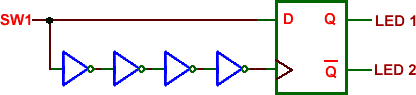
Now modify the circuit according to Fig. 11 by including four 7404 inverters to CLK. Repeat the above process. Can you explain why it is different now?
Fig. 10 Fig. 11
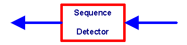
3.2. Sequence Detector
An application of sequential logic circuit is to implement finite state automaton. We will design an one-input, one output sequence detector which produces an output 1 everytime the sequence 0101 is detected, and an output 0 at all other times (see Fig. 12). Design and construct the sequence detector using D flip-flops.
0 0 0 1 0 1 .......
0 1 0 1 0 1...... Fig. 12. Sequence detector.
4. Prelab Assignment
For the sequence detector:
1. Obtain the state diagram of the sequence detector.
2. Derive the transition and output tables.
3. Derive the excitation and output functions.
4. Draw the circuit diagram of the sequence detector.
5. Equipment and parts needed
• Protoboard
• One TTL inverter (7404)
• One TTL NOR (7402)
• One TTL NAND (7400)
• Two D Flip-Flops (7474)