|
Go to ECE394 Experiment | 1 | 2 | 3 | 4 | 5 | 6 | 7 | 8 | 9 | Lab manuals | ECE Lab home |
|
ECE 394 - Digital Systems Laboratory
Experiment 1
Logic Gates and Logic Families
1. Introduction
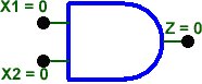
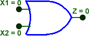
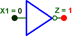
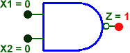
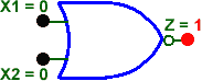
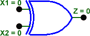
The basic logic gates are the basic building blocks of more complex logic circuits. These logic gates perform the basic Boolean functions, such as AND, OR, NAND, NOR, Inversion, Exclusive-OR, Exclusive-NOR. Fig. 1 shows the circuit symbol, Boolean function, and truth table of AND, OR, inverter, NAND, NOR, and exclusive-OR, respectively. You can see from Fig. 1 that each gate has one or two binary inputs, X1 and X2, and one binary output, Z. The small circle on the output of the circuit symbols designates the logic complement. The AND, OR, NAND, and NOR gates can be extended to have more than two inputs. A gate can be extended to have multiple inputs if the binary operation it represents is commutative and associative.
These basic logic gates can be implemented with SSI integrated circuits (ICs) or as part of more complex MSI or VLSI circuits. Digital IC gates are classified not only by their logic operation, but also the specific logic-circuit family to which they belong. Each logic family has its own basic electronic circuit upon which more complex digital circuits and functions are developed. The following logic families are the most frequently used.
| TTL | ECL | MOS | CMOS |
| Transistor-transistor logic | Emitter-coupled logic | Metal-oxide semiconductor | Complementary metal-oxide semiconductor |
TTL and ECL are based upon bipolar transistors. TTL has a well established popularity among logic families. ECL is used only in systems requiring high-speed operation. MOS and CMOS, are based on field effect transistors. They are widely used in large scale integrated circuits because of their high component density and relatively low power consumption. CMOS logic consumes far less power than MOS logic.
There are various commercial integrated circuit chips available. TTL ICs are usually distinguished by numerical designation as the 5400 and 7400 series. The former has a wide
|
Name |
Circuit Symbol |
Truth Table |
Equations |
|||||||||||||||
|
AND |
|
|
|
|||||||||||||||
|
OR |
|
|
Z = X1 + X2 |
|||||||||||||||
|
NOT |
|
|
|
|||||||||||||||
|
NAND |
|
|
|
|||||||||||||||
|
NOR |
|
|
|
|||||||||||||||
|
EXCLUSIVE OR |
|
|
Z = X1 Å X2 |
|||||||||||||||
operating-temperature range, suitable for military use, and the latter has a narrower temperature range, suitable for industrial use. The power supply for TTL ICs usually is 5V. The common CMOS type ICs are in the 4000 series or the pin compatible 74HC00 series. The power supply for CMOS ICs ranges from 3V to 15V. The common ECL type is designated as the 10,000 series.
Each logic family is characterized by several circuit parameters.
Fan-out specifies the number of standard loads that the output of a gate can drive without impairing its normal operation. A standard load is usually defined as the amount of current needed by an input of another gate in the same logic family. Sometimes, the term loading is used instead of fan-out. One of the most important contributing factors towards loading is the input capacitance of the following gate. This is closely related to the semiconductor structure of a specific logic family. For instance, the standard TTL gate will typically have a maximum fan-out of 50. Exceeding the specified maximum fan-out (or load) may cause a malfunction because the circuit cannot supply the power demanded from it.
Power dissipation is the supplied power required to operate the desired logic function. This parameter does not include the power delivered from another gate. Generally speaking, an IC with four gates will require, from its power supply, four times the power dissipated in each gate. Power dissipation is an important parameter. A complex electronic system may have many thousands of gates. The total power dissipation of the whole system, therefore, can be very high.
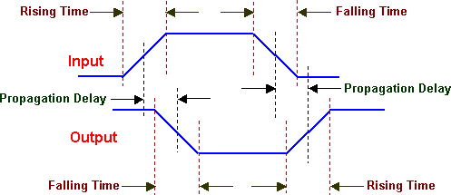
Propagation delay is the time delay for a signal transition to propagate from input to output when the binary input signals change in value. The signals passing through a gate take a certain amount of time to propagate from its inputs to the output. This interval of time is defined as the propagation delay of the gate. Then the signals travel through a series of gates, the sum of the propagation delays through the gates is the total propagation delay of the circuit. Both input and output signals are not ideal signals, i.e. they have finite rise and fall times (see Fig. 2). Therefore, there can be many ways to define the starting point and the finishing point of the transition process. Generally speaking, the starting point of the transition process depends upon the threshold point of the gate in question, and the finishing point of the transition process depends upon the threshold point of the following gate. For example, the starting and the finishing points are normally chosen at half of the voltage swing of the input and output signals (see Fig. 2). It should be noted that the transition period for the rising and falling edges of the same gate may not necessarily be the same, although it is normally desirable to have a symmetrical transition.
|
|
|
Fig. 2. Input output relationship. |
Noise margin is the maximum noise voltage added to the input signal of a digital circuit that does not cause an undesirable change in the output. There are two types of noise to be considered. DC noise is caused by a drift in the voltage levels of a signal. AC noise is a random pulse that may be created by other switching signals. Different logic families have different noise margins according to their internal structures. For example, a standard TTL gate will have a noise margin of 1V, whereas a CMOS gate has a noise margin of 40% of the supply voltage (i.e. if VDD = 5V, its noise margin is 2V).
2. Objectives
The objective of this lab is to introduce the concept of some basic logic gates and their dynamic characteristics. Students should become familiar with these characteristics. Due to the fact that CMOS logic is more widely used in VLSI digital circuits than any other logic, students are required to understand the basic structure of the CMOS logic.
3. Experiments
3.1 CMOS Inverter
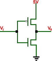
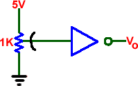
Fig. 3 shows a CMOS inverter circuit. It is made up of a p-type MOS transistor and a n-type MOS transistor. The 4069 contains 6 of these inverters on one chip. Connect one of the inverters as shown in Fig. 4. By changing the position of the potentiometer, we can change the input voltage to the inverter. Draw an input versus output curve with the input ranging from 0V to 5V. Suppose logic 0 is 0V and logic 1 is 5V, ideally. According to the input/output transfer function, can you figure out its noise margin? Now apply a square wave to the input of the inverter. Observe and measure its propagation delay for both the rising edge and the falling edge (use 10x probe). Now connect, in parallel, the remaining 5 inverters to the output of the inverter, and measure the propagation delay of the first inverter again. Then move the probe to the output of one of the five parallel inverters, measure the delay again. Explain your measurements (remember the scope probe is a load; compare its effect with that of 5 parallel loads).
Fig. 3. CMOS inverter. Fig. 4. Circuit for measuring I/O relation. 3.2. CMOS NAND Gate
Fig. 5 shows a two-input CMOS NAND gate circuit. Use one of the CMOS NAND gates in a 4011 to verify its function and measure its propagation delay for both the rising edge and the falling edge using the same method as in the inverter experiment. Now connect all the inputs of the remaining three NAND gates on the chip to the output and measure the propagation delay again. Explain your result.
3.4. CMOS AND Gate
Now that you are able to use the NAND and inverter to construct an AND gate. Try it. Draw a truth table to verify the function. Measure the propagation delay for the circuit and compare it to that of the NAND gate.
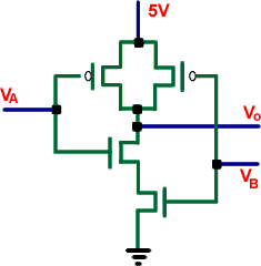 |
| Fig. 5. CMOS NAND gate. |
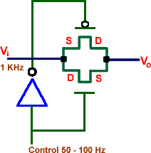
3.4. CMOS Transmission Gate
Fig. 6 shows a CMOS transmission gate circuit. Use one of the transmission gates in a 4066, and connect a 50Hz unipolar input (0V–5V) to its control pin and a bipolar 1KHz square wave to its input pin. Observe the output on a scope. Now change the control signal to a 50Hz bipolar input (+5V, -5V). What do you observe ? Can you explain the results?
Fig. 6. CMOS Transmission gate.
4. Equipment and parts required.
• One CMOS Inverter (4069)
• One CMOS NAND (4011)
• One CMOS Transmission Gate (4066)
• Two signal generators
• Multimeter