|
Go to ECE394 Experiment | 1 | 2 | 3 | 4 | 5 | 6 | 7 | 8 | Lab manuals | ECE Lab home |
|
ECE 394 -Digital Systems Laboratory
Experiment 9
Design Project – 4-bit RPN Calculator
1. Objectives
This project is designed to allow students to apply digital design techniques discussed in the previous experiments. The objective is to design a four-bit reverse polish notation (RPN) calculator. The components used consist of counters, multiplexers, 16¥4 RAMs, 4-bit ALU and PLD.
2. Requirement
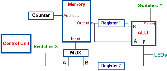
Fig. 1 shows the block diagram design of the calculator. The 16¥4 RAM serves as the stack of the RPN calculator and a four bit up/down counter is used as the stack pointer. Data can be entered into the stack through the switches X. To perform a calculation, the operands are first pushed into the stack and the desired function is selected with switches Y. The control unit of the calculator then goes through a sequence of steps to perform the operation. The final result is stored back into the RAM. The sequence of events that happens for each operation is as follows:
|
|
| Fig. 1. Block diagram design of a 4-bit RPN calculator. |
PUSH – push an operand into the stack.
Data are selected with switches X.
1. Increment the counter.
2. Write data into the memory.
FUNCTION – perform a calculation.
The function to be performed is selected with switches Y.
1. Data from RAM output is latched into register 1
2. Decrement the counter.
3. Result is latched into register 2.
4. Write data into the memory.
The control signals which are generated by the control unit are listed in Table 1.
| Table 1. Control signals for RPN calculator. | ||||||||
| Counter | Memory | Register1 | Register2 | ALU | MUX | Operation | ||
| Up | Down |
|
|
Enable | Enable | Select | Select | |
| 1 | 0 | 0 | 1 | 0 | 0 | * | * | PUSH |
| 0 | 0 | 0 | 0 | 0 | 0 | * | A | |
| 0 | 0 | 0 | 1 | 0 | 0 | * | A | |
| 0 | 0 | 0 | 1 | 1 | 0 | function | * | FUNCTION |
| 0 | 1 | 0 | 1 | 0 | 1 | function | * | |
| 0 | 0 | 0 | 0 | 0 | 0 | function | B | |
| 0 | 0 | 0 | 1 | 0 | 0 | function | B | |
Note. This table is just for reference, you should decide the exact signals according to what kind of chips you use.
The control circuit can be implemented by a state machine, memory lookup table, or can be generated using a PLD. Either design is acceptable.
3. Prelab Assignments
1. Design the control unit that would generate the control signals shown in Table 1.
2. Draw a circuit diagram of the calculator showing the connections for all the components.