Go to EE395 Experiment 1 2 3 4 5 Microprocessor board 8251A Interface SBC EEPROM ECE Lab home
![]()
|
Go to EE395 Experiment 1 2 3 4 5 Microprocessor board 8251A Interface SBC EEPROM ECE Lab home |
|
Appendix
Optional Parallel Port Expansion
Introduction
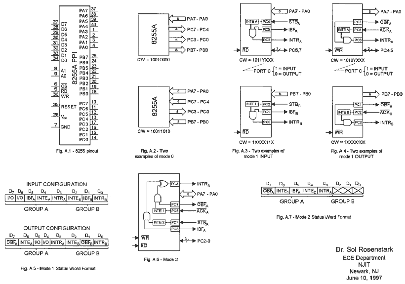
The parallel interface discussed so far was based on the 74373 and the 74244 chips. That is an inflexible design inasmuch as the direction of the ports cannot be changed and also because no handshaking features are available. If additional parallel interface capability is required then it is better to add a chip that has the features which were missing in the previous design. The Intel 8255A Programmable Peripheral Interface (PPI) packs a lot of versatile parallel interface into one 40-pin chip. Its pinout is shown in figure A.1.
The PPI has 24 pins of parallel I/O which can be configured in many different ways. These pins are divided into two basic groups, group A and group B. Group A consists of port A and the upper part of port C (bits 4 - 7). Group B consists of port B and the lower part of port C (bits 0 - 3). The assignment of the pins of port C to the two groups changes slightly with the modes of operation.
The ports of this chip can be operated in a number of different modes. In mode 0 the port A, port B, and the two halves of port C can be set up individually for either input or output. In mode 1 each group can be set up for either strobed input or strobed output, with some pins of port C used for handshaking. In mode 2, which is only available in group A, port A can be used for strobed bidirectional data transfer, with 5 pins of port C used for handshaking.
Interfacing to the CPU
The PPI can be interfaced to either 8-bit or 16-bit CPUs. It is easiest to discuss the operation of the PPI in connection with an 8-bit CPU. The question of how this chip is interfaced with a 16-bit CPU, such as the Motorola 68EC000 operating in 16-bit mode, is left as an exercise to the reader.
The PPI has 8 bidirectional data pins, D0 - D7, which are connected directly
|
Table 1 — Decoding Table for the PPI |
||
| Register | Pin Designation | Address |
|
Port A |
PA0 – PA7 PB0 – PB7 PC0 – PC7 . |
8000H 8001H 8002H 8003H |
to the CPU data bus. This chip
has separate ![]() and
and ![]() pins, which in our microprocessor
project would be interfaced with the two signals with that same designation,
derived from the 74LS32 OR-gates. The RESET pin would be tied to
the RESET signal used for the 8251A serial interface chip.
pins, which in our microprocessor
project would be interfaced with the two signals with that same designation,
derived from the 74LS32 OR-gates. The RESET pin would be tied to
the RESET signal used for the 8251A serial interface chip.
The chip select signal
![]() can
be connected to one of the 74LS138 decoder outputs. If it
were tied to the output
can
be connected to one of the 74LS138 decoder outputs. If it
were tied to the output ![]() then it would be decoded starting at 8000
H. The device has two pins marked A0 and A1. With our CPU these pins can
be connected to the correspondingly marked CPU address bus pins. The PPI
is then addressed according to the decoding table above.
then it would be decoded starting at 8000
H. The device has two pins marked A0 and A1. With our CPU these pins can
be connected to the correspondingly marked CPU address bus pins. The PPI
is then addressed according to the decoding table above.
Selecting the Operating Modes of the PPI
As mentioned in the introduction, the ports of the PPI are divided into two groups. Port A and the upper part of port C (bits 4 - 7) belong to group A. Port B and the lower part of port C (bits 0 - 3) belong to group B. The association of the parts of port C to the two groups is rather loose and bit 3 is shifted to group A when that group is used in mode 1 or mode 2.
Assigning Modes and Port Directions
The device can be operated in three modes. The modes of operation are selectable by writing a control byte to the CWR register. The bits of the control byte have a specific grouping. The control byte bits, designated
D7, D6, D5, D4, D3, D2, D1, D0
are used to select the following modes of operation:
D7 is the mode set flag. It must be 1 to activate mode setting.
D6, D5 are used to select the mode of operation of group A. They are used as follows:
D6, D5 = 00 selects mode 0.
D6, D5 = 01 selects mode 1.
D6, D5 = 1X selects mode 2.
D4 determines the direction of port A. Input = 1 and Output = 0.
D3 determines the direction of the upper half of port C. Input = 1 and Output = 0.
D2 is used to select the mode of operation of group B. D2 = 0 selects mode 0 and D2 = 1 selects mode 1. This group has no mode 1.
D1 determines the direction of port B. Input = 1 and Output = 0.
D0 determines the direction of the lower half of port C. Input=1 and Output=0.
Individual Bit Set / Reset Capability of Port C
In setting the mode of operation of the PPI we needed to write to the CWR using D7 = 1. Writing to the CWR with D7 = 0 can be used to set or reset specific bits of port C, one bit at a time. This assumes that port C is being used for output and not for input. If a group is in mode 0 then its portion of port C can be written to directly. In the two other modes the only way to change the output bits of port C is to use the bit set / reset method mentioned above.
To use the port C individual bit set / reset method, the control byte bits, designated
D7, D6, D5, D4, D3, D2, D1, D0
are used as follows:
We need D7 = 0 for port C bit setting to take place.
D6, D5 and D4 are "don’t cares."
D3, D2 a nd D1 determine which bit of port C will be affected, with 000 designating bit 0, 001 designating bit 1 and so on.
The value of D0 determines the value that the bit will take.
It should be noted that when ports are used for output, the last value written to them can be read back. This does not apply to the CWR.
The Operating Modes of the PPI
In the previous section it was explained how to obtain the various modes of operation. Now we need to become familiar with how those modes affect the operation of the ports of the PPI. But before we proceed, a few important observations are in order.
If any group is programmed in mode 0 for output, then the data can be sent to those pins by simply writing to port C. This is not true if a group is programmed in any mode other than mode 0. If it is desired to write any data to port C, when the group to which that port belongs is in mode 1 or 2, then this must be done on a bit by bit basis using the bit set/reset method. Hence if pins PC6,7 are used for output, in one of the two higher modes, then the data must be sent to them using the bit set/reset method.
In any mode, if any pins of port C are used for input then the data can be obtained by simply reading port C.
Mode 0 — Simple Input / Output
In mode 0 the ports are used for input or output without any handshaking. As an example, writing the control word CW = 10010000 to the CWR will cause mode setting to take place, and configure group A for input in mode 0. The upper part of port C will be configured for output. This CW will also configure group B for output in mode 0. The lower part of port C will be configured for output. This port configuration is demonstrated in figure A.2.
As another example, writing the control word CW = 10011010 to the CWR will configure group A for input in mode 0. The upper part of port C will also be configured for input. Group B will also be configured for input in mode 0. The lower part of port C will be configured for output. This port configuration is also demonstrated in figure A.2.
Mode 1 — Strobed Unidirectional Data Transfer
In mode 1 the ports are used for input or output with handshaking. If one group is used in mode 1, the other group can be used in any available mode. In mode 1 the five pins PC3-7 are assigned to group A. This leaves PC0-2 of port C assigned to group B. In figure A.3 we see how to configure group A and group B in mode 1 for input. In figure A.4 we see how to configure group A and group B in mode 1 for output. It is important to note that if group A is used on mode 1, then two pins of this group are left over for simple I/O. When group B is used in mode 1, however, then the three pins of lower port C are all assigned to handshaking duty. This is clearly demonstrated in figures A.3 and A.4.
The handshaking for the upper diagrams of figure A.3 and figure A.4 will be explained in detail. The other two cases can then be understood without further explanation.
When group A is used for input
in mode 1, as is the case for the upper diagram in figure
A.3, then the external device checks the "Input Buffer Full"
pin, IBFA. If this pin is low, indicating that the input buffer is empty, then the
external device puts a byte on pins PA7-PA0 and strobes it in by
momentarily pulling down the ![]() A
pin. The IBFA goes high
and stays in that state until the data is read by the CPU.
If the INTE A bit is set then the INTRA pin also goes
high. This can be used to interrupt the CPU and to inform it to call an interrupt
routine to read port A. The INTRA stays high until the data is read by
the CPU at which point the input cycle can be repeated.
A
pin. The IBFA goes high
and stays in that state until the data is read by the CPU.
If the INTE A bit is set then the INTRA pin also goes
high. This can be used to interrupt the CPU and to inform it to call an interrupt
routine to read port A. The INTRA stays high until the data is read by
the CPU at which point the input cycle can be repeated.
The CPU can keep itself informed of the progress of the data transfer by reading port C. The bit patterns for INPUT and OUTPUT are shown in figure A.5. If the IBF bit is set then the CPU knows that a new byte is waiting in the input buffer and that it can be read.
When group A is used for
output in mode 1, as is the case for the upper diagram in
figure A.4, the CPU reads the status word in port C and determines if
the "Output Buffer Full" ![]() A
bit is inactive high. If that is the
case then it can write a byte to port A. This causes the
A
bit is inactive high. If that is the
case then it can write a byte to port A. This causes the ![]() A status bit to become active low signaling the CPU
that the port A buffer is full. In addition the
A status bit to become active low signaling the CPU
that the port A buffer is full. In addition the ![]() A pin on
the PPI goes low.
A pin on
the PPI goes low.
The external device checks the
![]() A pin. If this pin is low, indicating that the output
buffer is full, then the external device reads the data and momentarily strobes
low the
A pin. If this pin is low, indicating that the output
buffer is full, then the external device reads the data and momentarily strobes
low the ![]() A pin. In response to this the
A pin. In response to this the
![]() A pin goes high informing
the peripheral that there is no new data for it to read. The corresponding
A pin goes high informing
the peripheral that there is no new data for it to read. The corresponding ![]() A
status bit also goes high informing the CPU that the data
has been read by the peripheral. If the INTE A bit is set
then the INTRA pin also goes high. This can be used to
interrupt the CPU and to inform it to call an interrupt
routine to send a new byte to port A.
A
status bit also goes high informing the CPU that the data
has been read by the peripheral. If the INTE A bit is set
then the INTRA pin also goes high. This can be used to
interrupt the CPU and to inform it to call an interrupt
routine to send a new byte to port A.
In figures A.3 and A.4 the INTE flip-flops are shown connected with dashed lines to the bit in port C that controls them. Thus, for setting INTE A, for the case shown in the upper diagram of figure A.3, it is necessary to use the bit set feature of the CWR to write a 1 to PC4. Reading of port C produces the status information shown in figure A.5 and the status of the INTE bits can be verified this way.
Mode 2 — Strobed Bidirectional Data Transfer
Mode 2 can be used only for group A for bidirectional data transfer with full handshaking. Group B can be used in mode 0 or mode 1 at the same time. The utilization of the pins is demonstrated in figure A.6. Careful examination of this figure reveals that it is composite of the upper two diagrams of figures A.3 and A.4. The handshaking which was explained for mode 1 applies here as well. The only difference is that there are two INTE flip-flops for the INTRA pin. One controls the interrupt enabling for output, the other for input.
As in the case of mode 1, reading of port C produces the status information shown in figure A.7. If interrupts are used for both input and output, the fact that there is only one INTRA pin means that the CPU must consult the status word to determine whether an input or output should be performed.
|
Go to EE395 Experiment 1 2 3 4 5 Microprocessor board 8251A Interface SBC EEPROM ECE Lab home |
|