Go to ECE489 Experiment | 1 | 2 | 3 | 4 | 5 | 6 | 7 | 8 | 9 | 10 | 11 | 12 | 13 | ECE Lab home
![]()
|
|
Go to ECE489 Experiment | 1 | 2 | 3 | 4 | 5 | 6 | 7 | 8 | 9 | 10 | 11 | 12 | 13 | ECE Lab home |
|
ECE 489 Communications Systems Laboratory
Experiment 14: BPSK - Binary Phase Shift Keying
ACHIEVEMENTS: Generation of binary phase shift keyed (BPSK) signal; bandlimiting; synchronous demodulation - phase ambiguities.
PREREQUISITES: It would be advantageous to have completed some of the experiments in Volume A1, involving linear modulation and demodulation. Familiarity with the DECISION MAKER, LINE- CODE ENCODER and LINE-CODE DECODER modules is assumed.
EXTRA MODULES: DECISION MAKER, LINE-CODE ENCODER and LINE-
CODE DECODER. A total of two PHASE SHIFTER modules is required.
Consider a sinusoidal carrier. If it is modulated by a bi-polar bit stream according to the scheme illustrated in Figure 1 below, its polarity will be reversed every time the bit stream changes polarity. This, for a sinewave, is equivalent to a phase reversal (shift). The multiplier output is a BPSK*(also sometimes called PRK - phase reversal keying) signal.
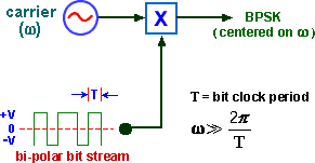 |
| Figure I: generation of BPSK |
The information about the bit stream is contained in the changes of phase of the transmitted signal.
A synchronous demodulator would be sensitive to these phase reversals.
The appearance of a BPSK signal in the time domain is shown in Figure 2 (lower trace). The upper trace is the binary message sequence.
 |
| Figure 2: a BPSK signal in the time domain. |
There is something special about the waveform of Figure 2. The wave shape is 'symmetrical' at each phase transition. This is because the bit rate is a sub-multiple of the carrier frequency w / (2p). In addition, the message transitions have been timed to occur at a zero-crossing of the carrier.
Whilst this is referred to as 'special', it is not uncommon in practice. It offers the advantage of simplifying the bit clock recovery from a received signal. Once the carrier has been acquired then the bit clock can be derived by division.
But what does it do to the bandwidth ?See Tutorial Question Q4.
The basic BPSK generated by the simplified arrangement illustrated in Figure 1 will have a bandwidth in excess of that considered acceptable for efficient communications.
If you can calculate the spectrum of the binary sequence then you know the bandwidth of the BPSK itself. The BPSK signal is a linearly modulated DSB, and so it has a bandwidth twice that of the baseband data signal from which it is derived*(This assumes w > 2B).
In practice there would need to be some form of bandwidth control.
Bandlimiting can be performed either at baseband or at carrier frequency. It will be performed at baseband in this experiment.
Demodulation of a B:PSK signal can be considered a two-stage process.
Translation back to baseband, with recovery of the band limited message waveform
Regeneration from the
bandlimited waveform back to the binary message bit stream.
Translation back to baseband requires a local, synchronized carrier.
Stage 1
Translation back to baseband is achieved with a synchronous demodulator, as shown in Figure 3 below.
This requires a local synchronous carrier. In this experiment a stolen carrier will be used.
Carrier acquisition will be investigated in the experiment entitled DPSK - carrier acquisition and BER (within Volume D2 - Further & Advanced Digital Experiments)
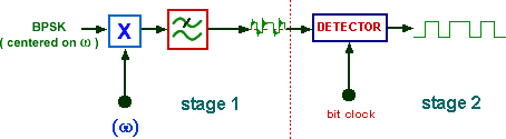 |
| Figure 3: synchronous demodulation of BPSK |
stage 2
The translation process does not reproduce the original binary sequence, but a band limited version of it.
The original binary sequence can be regenerated with a detector. This requires information regarding the bit clock rate. If the bit rate is a sub-multiple of the carrier frequency then bit clock regeneration is simplified.
In TIMS the DECISION MAKER module can be used for the regenerator, and in this experiment the bit clock will be a sub-multiple of the carrier.
You will see in the experiment that the sign of the phase of the demodulator carrier is important.
Phase ambiguity is a problem in the demodulation of a BPSK signal.
There are techniques available to overcome this. One such sends a training sequence, of known format, to enable the receiver to select the desired phase, following which the training sequence is replaced by the normal data (until synchronism is lost !).
An alternative technique is to use differential encoding. This will be demonstrated in this experiment by selecting a different code from the LINE-CODE ENCODER.
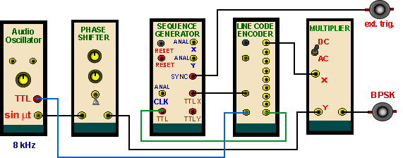
The BPSK generator of Figure 1 is shown in expanded form in Figure 4, and modeled in Figure 5
 |
| Figure 4: block diagram of BPSK generator to be modeled |
Note that the carrier will be four times the bit clock rate.
The lowpass filter is included as a band limiter if required. Alternatively a band pass filter could have been inserted at the output of the generator. Being a linear system, the effect would be the same.
 |
| Figure 5: model of the BPSK generator |
The AUDIO OSCILLATOR supplies a TTL signal for the bit clock digital DIVIDE- BY -FOUR sub-system in the LINE-CODE ENCODER, and a sinusoidal signal for the carrier.
The PHASE SHIFTER (set to the LO range with the on-board switch SW1) allows relative phase shifts. Watch the phase transitions in the BPSK output signal as this phase is altered. This PHASE SHIFTER can be considered optional.
The digital DIVIDE-BY-FOUR sub-system within the LINE-CODE ENCODER is used for deriving the bit clock as a sub-multiple of the BPSK carrier. Because the DECISION MAKER, used in the receiver, needs to operate in the range about 2 to 4 kHz, the BPSK carrier will be in the range about 8 to 16 kHz.
The NRZ-L code is selected from LINE-CODE ENCODER.
Viewing of the phase reversals of the carrier is simplified because the carrier and binary clock frequencies are harmonically related.
Tl Patch up the modulator of Figure 5; acquaint yourself with a BPSK signal. Examine the transitions as the phase between bit clock and carrier is altered. Vary the bandwidth of the PRBS with the TUNABLE LP F. Notice the envelope.
Figure 3 shows a synchronous demodulator for a BPSK signal in block diagram form. This has been modeled in Figure 6 below. In the first part of the experiment the carrier and bit clocks will be stolen.
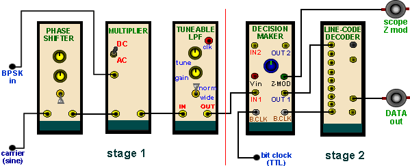 |
| Figure 6: the BPSK demodulator |
The phase of the carrier is adjustable with the PHASE SHIFTER for maximum output from the lowpass filter. Phase reversals of 1800 can be introduced with the front panel toggle switch.
Select the NRZ-L input to the LlNE-CODE DECODER. The LINE-CODE ENCODER and LINE-CODE DECODER modules are not essential in terms of the coding they introduce (since a bi-polar sequence is already available from the SEQUENCE GENERATOR) but they are useful in that they contain the DIVIDE-BY- FOUR sub-systems, which are used to derive the sub-multiple bit clock. .
The LPF following the demodulator multiplier is there to remove the components at double the carrier frequency. Its bandwidth can be set to about 12 kHz; although, for maximum signal-to-noise ratio (if measuring bit error rates, for example), something lower would probably be preferred.
The BPSK will have been bandlimited by the lowpass filter in the transmitter, and so the received waveform is no longer rectangular in shape. But you can observe that the demodulator filter output is related to the transmitted sequence (the NRZ-L code introduces only a level shift and amplitude scale).
The DECISION MAKER will regenerate the original TTL sequence waveform.
Notice the effect upon the recovered sequence when the carrier phase is reversed at the demodulator.
The following Tasks are a reminder of what you might investigate.
T2
Patch up the demodulator of Figure 6. The received signal will have come from the transmitter of
Figure 5. Observe the output from the
TUNABLE LP F, and confirm its appearance with respect to that transmitted. If the sequence is inverted then toggle the front panel 180ş switch of the receiver PHASE CHANGER.
T3
Set the on-board switch SW1 of the DECISION MAKER to accept NRZ-L coding. Use the gain control of the
TUNABLE LPF to set the input at about the TIMS ANALOG REFERENCE LEVEL of
±2 volt peak. Adjust the decision point. Check the output.
T4
Observe the TTL output from the LINE-CODE DECODER. Confirm that the phase of the receiver carrier (for the NRZ-L line code) is still important.
T5 Investigate a change of bandwidth of the transmitted signal. Notice that, as the bandwidth is changed, the amplitude of the demodulated sequence at the DECISION MAKER input will change. This you might expect; but, under certain conditions, it can increase as the bandwidth is decreased! How could this be ? See Tutorial Question Q6.
There is an extension to this experiment entitled DPSK -carrier acquisition and BER (within Volume D2 -Further & Advanced Digital Experiments)
Q1
Do you think BPSK is an analog signal ? Any comments ?
Q2 In the model of Figure 5, is it necessary that the MULTIPLIER be switched to DC, as shown?
Q3
You observed the shape of the phase transitions as the PHASE SHIFTER of Figure 5 was changed. Would this influence the spectrum of the
BPSK signal ?
Q4
Does making the bit rate a sub-multiple of the carrier frequency have any influence on the spectrum of the BPSK signal ?
Q5
What is the purpose of the lowpass filter in the BPSK demodulator model ? What determines its bandwidth ?
Q6
The amplitude of the signal at the DECISION MAKER input can decrease
as the bandwidth of the transmitter is widened
(or vice versa). At first glance this seems unusual ? Explain.
Q7 The PHASE SHIFTER in the demodulator of Figure 6 was adjusted for maximum output. What phase was it optimizing, and what was the magnitude of this phase ? Could you measure it ?
|
|
Go to ECE489 Experiment | 1 | 2 | 3 | 4 | 5 | 6 | 7 | 8 | 9 | 10 | 11 | 12 | 13 | ECE Lab home |
|